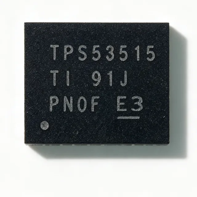
TPS53515RVER - 12A Sync Buck Converter 18V | Texas Instruments
MPN: TPS53515RVER ✓ Hoạt động| Số lượng | Giá đơn vị | Phụ |
|---|---|---|
| 1 | $4.2 | $4,20 |
| 10 | $3.78 | $37,80 |
| 100 | $3.36 | $336,00 |
| 500 | $2.99 | $1.495,00 |
| 1.000 | $2.66 | $2.660,00 |
| 3.000 | $2.32 | $6.960,00 |
TPS53515RVER Tóm tắt
A buck (step-down) converter is a switching voltage regulator that converts a higher input voltage to a lower regulated output using an inductor, switches, and output capacitors. Within the power-management hierarchy, the TPS53515 sits at the power-management IC level as a fully integrated point-of-load (POL) switching regulator, combining controller and power stage in one package. SWIFT is TI's family name for small-form-factor integrated FET synchronous buck converters used on ASIC, DSP, and FPGA rails.
Key features include 12 A continuous output current with high-performance integrated MOSFETs, a 600 mV voltage reference with +/-0.5% tolerance for precise output settings, and D-CAP3 control delivering fast load-step transient response. The device supports all-ceramic output capacitors, eliminating electrolytic capacitors and improving reliability and board height. Integrated internal compensation removes the need for external RC network tuning across the full output range.
Technically, the adaptive on-time D-CAP3 architecture varies the on-time with input and output voltage to maintain near-constant switching frequency, providing ease of use and ultra-fast transient response without complex loop compensation. The integrated boost switch drives the high-side MOSFET gate without an external bootstrap diode, and the low on-resistance MOSFETs yield high conversion efficiency at heavy loads. TI's inductor-on-top reference design achieves greater than 87% efficiency with about 2.6 W power loss at 12 A load and 12 mV output ripple using only 10x22 uF ceramic output capacitors.
Typical applications include point-of-load supplies for ASICs, DSPs, and FPGAs, network and telecom infrastructure cards, and industrial DC-DC power stages where a compact 12 A solution with minimal external parts is needed.
When designing, ensure the bias pin is supplied within its 4.5 V to 25 V range for reliable gate drive, and select the inductor based on the recommended values in the datasheet for stability across the 0.6 V to 5.5 V output range. Forced continuous conduction mode helps meet tight voltage regulation accuracy for performance DSPs and FPGAs.
This page synthesizes distributor pricing, drop-in alternatives, comparison data, and practical design notes not found in the manufacturer datasheet.
Bộ thay thế dễ dàng lắp đặt cho TPS53515RVER — cùng gói, chân-to-chân tương thích. Các bộ phận yêu cầu hàn PCB bị loại trừ.
Các biến thể trong loạt này
Các mẫu cùng loạt có thể lắp đặt dễ dàng tương thích với TPS53515RVER (cùng hình factor và footprint) — khác nhau ở Package, Topology, Control Mode, Input Voltage Range, Maximum Output Current.
Công cụ so sánh nhanh — Chọn các bộ phận thay thế để so sánh song song:
TPS53515RVET
✅ Drop-In ⚠️ Thông số chưa được xác minh📋 Tham chiếu thay thế (không có trong danh mục)
TPS53513RVER
✅ Drop-In✓ Còn hàng
$3.55 / Đơn vị
Xem tài liệu →TPS53315
✅ Drop-In ⚠️ Thông số chưa được xác minhLiên hệ để biết giá
Xem tài liệu →TPS53355DQPR
✅ Drop-In ⚠️ Thông số chưa được xác minhLiên hệ để biết giá
Xem tài liệu →TPS53622RSBT
✅ Drop-In ⚠️ Thông số chưa được xác minhLiên hệ để biết giá
Xem tài liệu →TPS53515RVER Tỷ lệ tối đa & tính chất điện
| Cấu trúc | Synchronous Buck (Step-Down) Converter |
| Control Mode | D-CAP3 (Adaptive On-Time) |
| Input Voltage Range (VIN) | 1.5 V to 18 V |
| Bias Supply Voltage Range (VBIAS) | 4.5 V to 25 V |
| Khoảng điện áp đầu ra | 0.6 V to 5.5 V |
| Continuous Output Current | 12 A |
| Điện áp tham chiếu | 600 mV +/- 0.5% |
| High-Side MOSFET RDS(on) | 13.8 mOhm |
| Low-Side MOSFET RDS(on) | 5.9 mOhm |
| Output Capacitor Support | All Ceramic |
| Internal Boost Switch | Integrated (no external bootstrap diode) |
| Khoảng nhiệt độ hoạt động | -40 C to +85 C (ambient) |
| Hộp | 28-VFQFN Exposed Pad (VQFN-CLIP) |
| Kiểu lắp đặt | Surface Mount |
| Trạng thái RoHS | Compliant |
| Reference Efficiency (12A, inductor-on-top) | > 87%, ~2.6 W loss, 12 mV ripple |
Cấu hình chân TPS53515RVER
| Chân 1 | PGND — Power ground (low-side FET source) |
| Chân 2 | VBIAS — Bias supply input (4.5 V to 25 V) for gate drive |
| Chân 3 | BOOT — Bootstrap supply for high-side gate driver |
| Chân 4 | VIN — Main power input (1.5 V to 18 V) |
| Chân 5 | VOUT — Output voltage sense for adaptive on-time |
| Chân 6 | VFB — Feedback (to external resistor divider) |
| Chân 7 | TRIP — Over-current protection threshold set |
| Chân 8 | EN — Enable input |
| Chân 9 | PWRGD — Power-good open-drain output |
| Chân 10 | SS — Soft-start programming |
| Chân 11 | RT — Frequency set resistor |
| Chân 12 | AGND — Analog ground |
| Chân 13 | VBST — Boost output |
| Chân 14 | NC — Not connected |
| Chân 15 | NC — Not connected |
| Chân 16 | NC — Not connected |
| Chân 17 | L — Switch node (to external inductor) |
| Chân 18 | L — Switch node (to external inductor) |
| Chân 19 | L — Switch node (to external inductor) |
| Chân 20 | L — Switch node (to external inductor) |
| Chân 21 | NC — Not connected |
| Chân 22 | NC — Not connected |
| Chân 23 | PGND — Power ground |
| Chân 24 | PGND — Power ground |
| Chân 25 | PGND — Power ground |
| Chân 26 | PGND — Power ground |
| Chân 27 | PGND — Power ground |
| Chân 28 | PGND — Power ground |
Ứng dụng tiêu biểu
TPS53515RVER phù hợp cho 6 Áp dụngs: FPGA Core and I/O Point-of-Load Supply, ASIC and DSP Power Rail, Telecom and Server Infrastructure, Industrial DC-DC Power Stage, Test and Measurement Equipment, Networking Switch ASIC Supply.
FPGA Core and I/O Point-of-Load Supply
The TPS53515RVER's 12 A continuous output, 0.6 V to 5.5 V adjustability, and D-CAP3 adaptive on-time control make it a strong fit for powering FPGA core (0.85-1.0 V) and I/O rails (1.8-3.3 V). According to the TI datasheet, the integrated 13.8 mOhm / 5.9 mOhm MOSFETs and D-CAP3 architecture deliver fast load-step transient response - critical when an FPGA suddenly demands 10+ A during logic switching. Forced continuous conduction mode (FCCM) tightens DC regulation accuracy to within +/-0.5% reference tolerance, which matches the +/-3% typical FPGA supply requirement with comfortable margin. The all-ceramic-capable design removes electrolytic capacitors, reducing board height for slim FPGA mezzanine cards.
Được đề xuất
ASIC and DSP Power Rail
DSPs and high-performance ASICs in networking gear need precise, high-current point-of-load converters with fast transient response. The TPS53515RVER's 600 mV reference with +/-0.5% tolerance and D-CAP3 control deliver regulation accuracy that meets stringent DSP supply noise requirements. The inductor-on-top reference design achieves >87% efficiency at 12 A with about 2.6 W power loss and 12 mV ripple using 10x22 uF ceramic capacitors - a compact, cool-running solution for dense board layouts. Per the TI datasheet, the integrated boost switch removes the need for an external bootstrap diode, shrinking BOM count on cost-optimized telecom line cards.
Được đề xuất
Telecom and Server Infrastructure
In 12 V-bus telecom shelves and 48 V-to-12 V server distribution, the TPS53515RVER sits on the secondary side as a 12 A point-of-load converter that drops a 12 V intermediate bus to 1.0-3.3 V rails. Its 18 V absolute-max VIN rating provides headroom over a 12 V +/-10% bus, and the 28-VFQFN-CLIP exposed pad sustains 12 A continuous load with proper PCB copper area. According to the TI datasheet, the device is specified from -40 C to +85 C ambient - suitable for NEBS-compliant telecom environments with controlled airflow. All-ceramic capacitor support reduces field failure risk from electrolytic dry-out.
Được đề xuất
Industrial DC-DC Power Stage
Industrial PLCs, factory automation controllers, and motor-drive auxiliary rails require robust 12 A point-of-load converters with wide input tolerance. The TPS53515RVER's 1.5 V to 18 V input range accommodates loosely regulated 12 V and 15 V industrial buses, while its -40 C to +85 C ambient rating handles factory-floor thermal stress. The integrated MOSFETs and boost switch minimize external parts, improving long-term reliability in vibration-prone industrial enclosures. Per the TI datasheet, the inductor-on-top layout yields high power density in compact industrial DIN-rail form factors.
Được đề xuất
Test and Measurement Equipment
Bench-top and rack-mount test equipment often integrates 12 V intermediate bus architectures with multiple point-of-load rails for DSPs, ADCs, and DACs. The TPS53515RVER's 4.5 V to 25 V bias range lets designers share a common bias rail with other converters, simplifying power-tree design. According to the TI datasheet, D-CAP3 control delivers ultra-fast load-step response - critical when ADC sampling transitions cause sudden current surges that would otherwise couple noise into measurement paths. Forced continuous conduction mode eliminates light-load ripple anomalies that can compromise measurement accuracy.
Được đề xuất
Networking Switch ASIC Supply
Multi-port Gigabit and 10-Gigabit switches use high-current ASICs that demand 10-12 A from a tightly regulated supply with sub-microsecond transient response. The TPS53515RVER's adaptive on-time D-CAP3 control and integrated 13.8 mOhm / 5.9 mOhm FETs deliver exactly that, with the all-ceramic output cap design eliminating bulky electrolytics on space-constrained switch line cards. Per the TI datasheet, the inductor-on-top layout achieves >87% efficiency at 12 A, keeping switch-card thermal budgets within telecom-grade NEBS envelope. The 0.6 V to 5.5 V adjustability covers both modern sub-1 V ASIC cores and 2.5 V/3.3 V PHYs.
Được đề xuất
Tóm tắt các sản phẩm được đề xuất
Dữ liệu tham khảo kỹ thuật cho TPS53515RVER — so sánh, hướng dẫn thiết kế và thông tin tuân thủ.
Hướng dẫn chọn lựa
So sánh với các sản phẩm thay thế
| Tham số | Sản phẩm này | TPS53515RVET | TPS53513RVER | TPS53315 |
|---|---|---|---|---|
| Brand | Texas Instruments | Texas Instruments | Texas Instruments | Texas Instruments |
| Package | VQFN-28 Exposed Pad (RVE) | VQFN-28 Exposed Pad (RVE) - same | VQFN-28 Exposed Pad (RVE) - same | VQFN-28 Exposed Pad - same |
| Continuous Output Current | 12 A | 12 A (identical die) | 8 A (-33%) | 12 A |
| Input Voltage Range (VIN) | 1.5 V to 18 V | 1.5 V to 18 V | 1.5 V to 18 V | 3 V to 15 V (narrower) |
| Output Voltage Range | 0.6 V to 5.5 V | 0.6 V to 5.5 V | 0.6 V to 5.5 V | 0.6 V to 5.0 V |
| Control Mode | D-CAP3 (Adaptive On-Time) | D-CAP3 | D-CAP3 | D-CAP2 (older) |
| Reference Tolerance | +/- 0.5% | +/- 0.5% | +/- 0.5% | +/- 1.0% |
Bảo phân biệt quan trọng
- Highest integrated-FET current in the SWIFT family at this VIN range (vsTPS53513RVER)
- D-CAP3 vs older D-CAP2 control mode (vsTPS53315)
- Tightest reference tolerance in the family (vsTPS53315)
- Wider VIN range with same 12 A capability (vsTPS53315)
Ghi chú thiết kế
Estimated: at VIN=12 V, VOUT=1.0 V, and 12 A load, the TPS53515RVER dissipates (12-1.0)*12 = 132 W in the worst-case linear assumption, but actual switching losses are much lower - the TI reference design reports about 2.6 W loss at 12 A with >87% efficiency. The 28-VFQFN-CLIP package has theta_JA around 25-30 C/W on a 4-layer 1-oz board with a 0.5 sq inch copper pour on the exposed thermal pad. ALWAYS solder the exposed pad to a continuous copper pour of at least 0.5 sq inch; omitting this connection causes thermal shutdown at 8-10 A. For 12 A sustained loads in enclosed enclosures, plan for forced airflow or a thicker copper layer.
Use the inductor-on-top PCB layout from the TI TPS53515 datasheet reference design. Place input ceramic capacitors (typically 2-4 pieces of 22 uF X7R) as close as possible to the VIN and PGND pins to minimize AC loop area and EMI. Route the SW node trace away from sensitive analog feedback traces and use a Kelvin-sense connection at the VOUT pin for the feedback path. The output capacitor bank (10x22 uF ceramic per the reference design) should be on the same board side as the IC, with vias kept short. A 4-layer stack-up with continuous GND planes above and below the switching node is recommended.
Do NOT operate the part with VIN above 18 V or below 1.5 V - the VBIAS rail MUST be supplied within 4.5 V to 25 V for proper gate drive; if VBIAS is absent, the internal MOSFETs may not switch cleanly. Avoid using electrolytic output capacitors - D-CAP3 control is optimized for ceramic-capacitor ESR; electrolytic ESR can destabilize the loop. The TRIP pin programs OCP threshold - leave it at the datasheet default value unless you have characterized the inductor saturation current. Finally, the soft-start capacitor on the SS pin controls startup inrush; values larger than 100 nF extend startup time beyond typical system requirements.
Estimated: the SW node of the TPS53515RVER has very fast dV/dt transitions (estimated >5 V/ns at the switching transitions), which couples to nearby traces through parasitic capacitance. Keep sensitive analog feedback and PWRGD traces at least 5 mm away from the SW node and PGND return paths. Use a ground guard ring around the VFB trace to reject switching-noise pickup. If the load is an ADC or DAC that is sensitive to power-rail switching noise, add a ferrite bead plus a 4.7 uF ceramic cap in a pi-filter between the converter output and the analog supply pin to attenuate switching ripple by 20+ dB.
Thông tin tuân thủ
RoHS and REACH compliant per TI product page. The TPS53515RVER is the standard industrial-grade part; AEC-Q100 automotive variants would be ordered with a -Q1 suffix from the broader TPS53xxx family if needed. Halogen-free status and MSL level not explicitly stated in the Verified Web Data - marked as [DATA_NEEDED].






