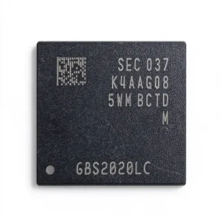
H5AN8G8NCJR-VKI - DDR4 8Gb 2666Mbps DRAM | SK hynix
MPN: H5AN8G8NCJR-VKI ✓ 啟用中H5AN8G8NCJR-VKI 概覽
DDR4 SDRAM is a synchronous dynamic random-access memory that transfers data on both clock edges (double data rate), providing high bandwidth for processors and SoCs. Within the memory hierarchy it sits as volatile main memory, below non-volatile flash storage and above cache, and is a core building block of power management and memory subsystem design in computing platforms.
Key features of the H5AN8G8NCJR-VKI include the 8Gb (1G x8) density, a 2666 Mbps data rate (PC4-21300 class), a 1.2 V core supply that reduces power versus DDR3's 1.5 V, and the compact 78-ball FBGA surface-mount package suited to dense memory layouts. The industrial operating range supports extended-temperature designs where commercial-only DRAM is unsuitable.
Technically, the part belongs to the H5AN8G8NCJR-xxC/xI DDR4 SDRAM family, which SK hynix documentation describes as an 8Gb CMOS Double Data Rate IV synchronous DRAM ideally suited for main memory applications requiring large memory density and high bandwidth. The x8 organization allows 78-ball packaging with fewer data lines per device, simplifying layout for 64-bit or ECC-enabled memory controllers.
Typical applications include industrial controllers, computing modules, networking equipment, servers, and embedded systems where stable DDR4 sourcing still matters. The industrial grade supports factory automation and edge-computing platforms exposed to harsher thermal environments.
When designing with this device, verify controller speed-grade compatibility (2666 Mbps), budget termination and VTT power for the DDR4 bus, and follow SK hynix layout guidance for fly-by clock routing and decoupling on the 1.2 V rail.
This page synthesizes distributor stock and pricing data, same-family and cross-brand drop-in alternatives, and practical design notes not found in the manufacturer datasheet.
直接替換替代品,適用於 H5AN8G8NCJR-VKI — 相同封裝,腳位對腳位相容。需重新設計 PCB 的不同封裝零件不列入。
此系列的變體
與下列產品可直接替換的同系列型號: H5AN8G8NCJR-VKI (相同外形與佔位) — 差異在於 Package, Data Rate, Interface, Memory Size, Organization.
H5AN8G8NCJR-VKC
✅ 直接替換聯絡詢價
查看資料表 →H5AN8G8NCJR-UHC
✅ 直接替換聯絡詢價
查看資料表 →H5AN8G8NCJR-RDC
✅ 直接替換聯絡詢價
查看資料表 →H5AN8G8NCJR-PBC
✅ 直接替換聯絡詢價
查看資料表 →MT40A1G8AG-062E
✅ 直接替換聯絡詢價
查看資料表 →K4A8G085WC-BCTD
✅ 直接替換聯絡詢價
查看資料表 →H5AN8G8NCJR-VKI 最大額定值與電氣特性
| 記憶體類型 | DDR4 SDRAM |
| 記憶體容量 | 8 Gb |
| Memory Organization | 1G x8 |
| 資料速率 | 2666 Mbps |
| 供應電壓 | 1.2 V |
| 介面 | Parallel |
| Memory Format | DRAM |
| Volatile | Yes |
| 封裝 | FBGA-78 |
| 安裝類型 | Surface Mount |
| Grade | Industrial (I suffix) |
| Technology | CMOS |
| Product Family | H5AN8G8NCJR-xxC/xI DDR4 SDRAM |
| Packaging | Tray |
| Product Status | Active |
H5AN8G8NCJR-VKI fbga-78 腳位配置指南
H5AN8G8NCJR-VKI(fbga-78 封裝)的腳位配置。 此數位 IC 包含 GPIO、通訊介面(UART、SPI、I2C)與電源腳位。替代腳位功能與配置選項請參閱製造商資料表。對嵌入式系統設計與 PCB 佈局至關重要。

無詳細腳位定義資料: H5AN8G8NCJR-VKI.
請參閱 資料表 以查看完整腳位配置。
典型應用
H5AN8G8NCJR-VKI 適用於 6 應用s: Industrial Controllers, Embedded Computing Modules, Networking Equipment, Server and Data Center Memory, Embedded Logging and Data Storage, Firmware Boot and Replacement Sourcing Platforms.
Industrial Controllers
Industrial programmable controllers and factory automation platforms require main memory that survives extended temperatures and continuous duty cycles. The H5AN8G8NCJR-VKI fits this role with its industrial (I) temperature suffix, 8Gb density per device, and 2666 Mbps bandwidth for real-time control code and data buffering. In a typical controller, two to four of these x8 devices populate a 64-bit or ECC-protected DDR4 channel fed by an industrial-grade SoC; the 1.2 V rail keeps DRAM power low inside sealed enclosures with limited airflow. Designers should confirm junction temperatures at maximum ambient and apply the fly-by clock topology recommended in the SK hynix datasheet to maintain signal integrity at full speed.
推薦
Embedded Computing Modules
COM Express and SMARC compute modules pack DRAM in tight z-heights, making the 78-ball FBGA package of the H5AN8G8NCJR-VKI ideal for solder-down memory on the module PCB. Its 1G x8 organization allows ECC-enabled module designs and flexible channel widths, while 2666 Mbps per pin supplies adequate bandwidth for edge-analytics and gateway workloads. Using solder-down DDR4 instead of SODIMMs improves vibration tolerance - critical for transportation and automation modules. Layout effort concentrates on length-matched fly-by routing and VTT termination; the compact FBGA keeps stubs short, helping designs meet eye-mask requirements at 2666 Mbps across the industrial temperature range.
推薦
Networking Equipment
Switches, routers, and network appliances need deep packet buffers and large table memory, where the H5AN8G8NCJR-VKI's 8Gb-per-device density and 2666 Mbps throughput deliver high aggregate bandwidth with modest chip counts. An x8 organization lets network processors build 72-bit ECC buses (64 data + 8 check) using nine devices. The 1.2 V supply helps control the power budget of fanless branch-office and industrial networking hardware. Because network gear runs 24/7 at elevated ambient inside racks, the industrial temperature grade of the VKI adds sourcing margin; pair it with a controller whose DDR4 PHY supports write-leveling and read-training to sustain link integrity at full data rate.
推薦
Server and Data Center Memory
Although high-volume servers typically buy registered DIMMs, appliance servers and storage nodes increasingly use solder-down DDR4 like the H5AN8G8NCJR-VKI for cost and density control on custom baseboards. The 8Gb 1G x8 device supports the x8-based ECC schemes standard in server memory controllers, and 2666 Mbps matches mainstream DDR4-2666 platform speeds. Its 1.2 V operation reduces per-GB power versus DDR3, easing rack thermal budgets. For appliance designs, the x8 organization also enables Post Package Repair and single-device data correction on supporting controllers - reliability features that matter for always-on storage and edge-datacenter deployments.
推薦
Embedded Logging and Data Storage
Storage appliances, RAID controllers, and industrial data loggers use DDR4 DRAM as write cache and buffering memory ahead of NAND. The H5AN8G8NCJR-VKI provides 8Gb of volatile buffering with 2666 Mbps bandwidth to absorb burst writes from gigabit-class interfaces, protecting NAND endurance by smoothing write amplification. Its industrial grade suits unattended edge logging in energy, transportation, and telecom infrastructure where ambient temperatures swing widely. Designers pair the DRAM with power-fail circuitry so buffered data flushes to NAND on outages; the x8 organization supports the ECC that makes cache data integrity auditable, and the FBGA package supports conformal-coated boards for harsh environments.
推薦
Firmware Boot and Replacement Sourcing Platforms
Beyond new designs, the H5AN8G8NCJR-VKI is widely referenced in replacement sourcing and repair of industrial computing hardware still shipping with DDR4-2666 x8 solder-down memory. Distributor listings (Octopart: ~40040 pcs; icDirectory: ~23350 pcs in 2026) show continued availability, making it a low-risk service part. Repair depots reball or machine-place the 78-ball FBGA on controller boards for embedded loggers, industrial PCs, and networking modules. When qualifying replacements, match the speed suffix (VKI = 2666 industrial) or verify a slower variant is accepted by the platform firmware, and source traceable stock to avoid remarketed or counterfeit DRAM in repaired units.
推薦
推薦產品摘要
工程參考資料,適用於 H5AN8G8NCJR-VKI — 比較、設計指引及合規資訊。
選型指南
與替代品比較
| 參數 | 本產品 | H5AN8G8NCJR-VKC | H5AN8G8NCJR-UHC | MT40A1G8AG-062E | K4A8G085WC-BCTD |
|---|---|---|---|---|---|
| Package | FBGA-78 | FBGA-78 - same | FBGA-78 - same | FBGA-78 - same (JEDEC DDR4 x8 ballout) | FBGA-78 - same (JEDEC DDR4 x8 ballout) |
| Brand | SK Hynix | SK Hynix | SK Hynix | Micron Technology | Samsung |
| Memory Size | 8 Gb | 8 Gb | 8 Gb | 8 Gb | 8 Gb |
| Organization | 1G x8 | 1G x8 | 1G x8 | 1G x8 | 1G x8 |
| Supply Voltage | 1.2 V | 1.2 V | 1.2 V | 1.2 V | 1.2 V |
| Lifecycle Status | Active | Active | Active | Active | Active |
主要差異化特點
- Industrial temperature grade at 2666 Mbps (對比H5AN8G8NCJR-VKC)
- Full 2666 Mbps data rate (對比H5AN8G8NCJR-UHC)
- Multi-vendor second sourcing (對比MT40A1G8AG-062E)
設計說明
At 2666 Mbps, DDR4 timing margins are tight. Route address/command lines in fly-by topology with length-matched stubs, keep DQ/DQS pairs length-matched within the tolerance specified in the SK hynix datasheet, and reference signals to solid ground planes. Enable the controller's write-leveling, read-training, and VREFDQ training algorithms during bring-up; skipping training is the most common cause of marginal DDR4 operation at full speed across temperature corners.
The H5AN8G8NCJR-VKI runs from a 1.2 V VDD rail with DDR4 also requiring VPP (~2.5 V) and a VTT termination rail tracking VDD/2. Size the VTT regulator for the bus termination current of your device count and confirm current consumption against the datasheet IDD tables for your access pattern. Estimated: a 64-bit bus with 8 x8 devices draws substantial transient termination current, so use plane pours and dense 100 nF + 10 uF decoupling at every device.
Verify speed and temperature suffixes when substituting within the H5AN8G8NCJR family: -VKI is 2666 Mbps industrial, -VKC is 2666 commercial, and -UHC/-RDC/-PBC are lower speed grades. Firmware and SPD/controller configuration must match the installed grade. Also source only traceable stock - commodity DDR4 is a frequent counterfeit target - and request date codes and certificates of conformance from the distributor.
合規資訊
Compliance data not present in the verified web data provided. Confirm RoHS/REACH status from the SK hynix product page or distributor compliance certificates before release.