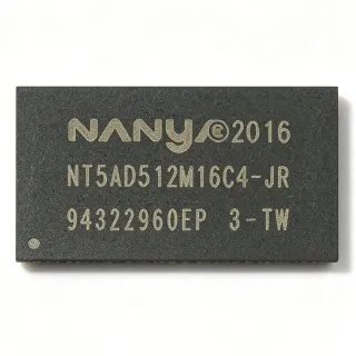
H5CG34MEBDX030 - DDR5 SDRAM DRAM Chip | SK hynix
MPN: H5CG34MEBDX030 ✓ 啟用中H5CG34MEBDX030 概覽
A DDR5 SDRAM is the fifth generation of double-data-rate synchronous dynamic random-access memory, the volatile memory class that sits at the top of the memory hierarchy in servers, PCs, and embedded systems. Compared with DDR4, DDR5 doubles the bank groups, moves the power management IC (PMIC) onto the module, lowers the per-cell operating voltage, and raises data rates beyond 4800 MT/s, making it the backbone technology for memory-intensive compute platforms.
Key characteristics of the H5CG DDR5 family include high-speed point-to-point data links, on-die ECC (link ECC with on-die error checking), a same-bank refresh (REFsb) capability that improves effective bandwidth, and burst length of 16 for improved bus efficiency. These features matter for AI accelerator memory, high-performance computing, and server main memory where bandwidth per watt is a key metric.
Architecturally, DDR5 devices split each rank into two independent 32-bit sub-channels with their own CA and CS signals, allowing two concurrent access streams and shorter burst lengths. Internal banks are wider and refresh schemes are more granular than DDR4, which raises effective throughput under mixed read/write workloads.
Typical applications include data-center server DIMMs and RDIMMs, desktop and workstation UDIMMs, AI/GPU accelerator memory subsystems, networking equipment buffers, and high-end embedded computing where DDR5 memory controllers (such as Intel or AMD server SoCs) are used.
Design consideration: DDR5 signal integrity demands length-matched routing, ODT (on-die termination) tuning, and correct VDDQ/VDD rail decoupling; always verify speed grade and CL timings against the controller's trained values.
This page adds value beyond the datasheet by aggregating drop-in alternatives, buying guidance, and practical DDR5 design notes in one place.
直接替換替代品,適用於 H5CG34MEBDX030 — 相同封裝,腳位對腳位相容。需重新設計 PCB 的不同封裝零件不列入。
此系列的變體
與下列產品可直接替換的同系列型號: H5CG34MEBDX030 (相同外形與佔位) — 差異在於 Data Rate, Interface Type, Organization, Density, Package.
H5CG44MEBDX014
✅ 直接替換 ⚠️ 規格未經驗證聯絡詢價
查看資料表 →H5CG44MEBDX014N
✅ 直接替換 ⚠️ 規格未經驗證聯絡詢價
查看資料表 →H5CG46MEBDX015N
✅ 直接替換 ⚠️ 規格未經驗證聯絡詢價
查看資料表 →H5CG48MEBDX014N
✅ 直接替換 ⚠️ 規格未經驗證聯絡詢價
查看資料表 →H5CG46MEBDX017N
✅ 直接替換 ⚠️ 規格未經驗證聯絡詢價
查看資料表 →H5CG26AGBDX021
✅ 直接替換 ⚠️ 規格未經驗證聯絡詢價
查看資料表 →H5CG28AGBDX022
✅ 直接替換 ⚠️ 規格未經驗證聯絡詢價
查看資料表 →H5CG34MEBDX030 規格
| Manufacturer | SK hynix |
| Product Family | H5CG (DDR5 SDRAM) |
| 記憶體類型 | DDR5 SDRAM |
| 封裝 | FBGA (fine-pitch BGA), surface mount |
| 安裝類型 | Surface Mount |
| On-die ECC | Yes (DDR5 standard feature) |
| Burst Length | 16 (DDR5 standard) |
| 介面類型 | Parallel, DDR5 point-to-point |
| RoHS 狀態 | Compliant |
H5CG34MEBDX030 fbga (fine-pitch bga), surface mount 腳位配置指南
H5CG34MEBDX030(fbga (fine-pitch bga), surface mount 封裝)的腳位配置。 腳位編號、功能與連接圖定義於製造商資料手冊中。請參閱該手冊以取得確切的封裝尺寸與焊接指引。

無詳細腳位定義資料: H5CG34MEBDX030.
請參閱 資料表 以查看完整腳位配置。
典型應用
H5CG34MEBDX030 適用於 6 應用s: Data-Center Server Main Memory, AI and Machine Learning Accelerators, Desktop and Workstation PCs, Networking and Telecom Equipment, Industrial Embedded Computing, Test and Measurement Instrumentation.
Data-Center Server Main Memory
The H5CG34MEBDX030 serves as core DDR5 SDRAM in server RDIMM, LRDIMM, and memory-down designs. SK hynix DDR5 components are used across hyperscale and enterprise platforms where the dual 32-bit sub-channel architecture and burst length 16 raise effective bandwidth per rank, while on-die ECC reduces silent data corruption risk. Placed on registered modules behind an RCD (registering clock driver), the device operates at DDR5-class voltage rails managed by the on-module PMIC. For server designs, verify speed bin and timing compatibility with the CPU memory controller's trained values, and follow SK hynix module reference designs for SPD hub and PMIC integration. Second-sourcing across SK hynix/Micron/Samsung JEDEC-compliant DDR5 parts is standard practice for supply resilience.
推薦
AI and Machine Learning Accelerators
AI training and inference boards require high-bandwidth main memory alongside HBM; DDR5 components like H5CG34MEBDX030 supply the host-side memory pool feeding accelerators. The DDR5 family's higher bank group count and REFsb (same-bank refresh) sustain effective throughput under the random access patterns typical of embedding lookups and KV-cache paging. In accelerator cards, DDR5 is often laid out memory-down close to the SoC, with length-matched fly-by routing and per-device ODT tuning. The on-die ECC feature is valued in long-running training jobs where an uncorrected DRAM bit flip can invalidate a multi-day compute run. Designers should budget power for VDDQ rail transients during simultaneous burst writes across multiple devices.
推薦
Desktop and Workstation PCs
Consumer and workstation platforms with Intel or AMD DDR5 memory controllers use H5CG-family SDRAM both on UDIMM modules and in memory-down motherboards. The H5CG34MEBDX030 provides the JEDEC DDR5 feature set including on-die ECC and burst length 16 that raise effective bandwidth for gaming and content-creation workloads. On client platforms, memory training at each boot programs ODT, drive strength, and timing registers, so substitute parts must match speed bin and density to avoid retraining failures. Thermal design on close-spaced DIMMs should keep device case temperature within the datasheet operating range under sustained memory bandwidth loads. XMP/EXPO profiles above JEDEC timings should be validated per platform QVL.
推薦
Networking and Telecom Equipment
Routers, switches, and 5G baseband units buffer packets and flow tables in DDR5 memory; H5CG34MEBDX030 fits these designs with its point-to-point DDR5 interface and sustained random-access efficiency from expanded bank groups. Networking workloads stress random read/write alternation, where DDR5's shorter bursts and dual sub-channels outperform DDR4 at equivalent bus widths. Telecom platforms often demand industrial temperature ranges and long lifecycle supply, so verify the temperature grade in the SK hynix ordering code and qualify the device at corner temperatures during bring-up. Power-sensitive line-card designs benefit from DDR5's lower core voltage relative to DDR4, reducing memory-subsystem wattage at equivalent bandwidth.
推薦
Industrial Embedded Computing
Industrial PCs, edge AI gateways, and machine-vision controllers use DDR5 SDRAM such as H5CG34MEBDX030 for high-bandwidth frame buffers and inference workloads. Embedded designs frequently mount DRAM memory-down directly on the CPU board, so PCB stack-up, fly-by routing topology, and reference plane integrity follow Intel/AMD DDR5 layout guides alongside SK hynix package outline data. The on-die ECC feature adds robustness for always-on edge systems in electrically noisy factory environments. Designers should confirm the industrial operating temperature option in the part ordering code, since commodity DRAM defaults to a commercial range, and specify conformal-coating-compatible cleaning processes given the fine-pitch FBGA ball pitch.
推薦
Test and Measurement Instrumentation
High-channel-count oscilloscopes, logic analyzers, and signal generators capture enormous waveform datasets that stream into DDR5 memory; the H5CG34MEBDX030 provides the sustained write bandwidth and capacity these instruments require. DDR5's dual sub-channel architecture lets instrument SoCs run independent capture and analysis streams concurrently, improving real-time trigger-to-display latency. In instrument designs, DDR5 is typically memory-down with aggressive signal-integrity engineering: on-die termination tuning, per-byte lane deskew, and rigorous IBIS/S-parameter channel simulation before tape-out. On-die ECC protects long captures from silent corruption, which matters for compliance-grade measurements where data integrity is auditable. Verify JEDEC speed-bin timing closure with the instrument SoC's memory controller during design validation.
推薦
推薦產品摘要
工程參考資料,適用於 H5CG34MEBDX030 — 比較、設計指引及合規資訊。
選型指南
與替代品比較
| 參數 | 本產品 | H5CG44MEBDX014 | H5CG44MEBDX014N | H5CG46MEBDX015N | H5CG48MEBDX014N |
|---|---|---|---|---|---|
| Package | FBGA | FBGA - same | FBGA - same | FBGA - same | FBGA - same |
| Brand | SK hynix | SK hynix | SK hynix | SK hynix | SK hynix |
| Memory Type | DDR5 SDRAM | DDR5 SDRAM | DDR5 SDRAM | DDR5 SDRAM | DDR5 SDRAM |
| Family | H5CG DDR5 | H5CG DDR5 | H5CG DDR5 | H5CG DDR5 | H5CG DDR5 |
| On-die ECC | Yes | Yes | Yes | Yes | Yes |
主要差異化特點
- SK hynix in-house DRAM process with mature DDR5 yield (對比H5CG44MEBDX014N)
- Native DDR5 feature set (on-die ECC, BL16, dual 32-bit sub-channels) (對比H5ANAG8NBJR-RDC)
- Second-source coverage within one vendor family (對比H5CG46MEBDX015N)
設計說明
DDR5 fly-by routing requires strict length matching within each byte lane group and controlled impedance (typically 40 ohms single-ended for CA/DQ). Keep the FBGA breakout region short - route stubs under 50 mils where possible - and reference DQ signals to a continuous VDDQ plane. Simulate the full channel with SK hynix IBIS models and the memory controller's SSTL/Pseudo-Open-Drain driver models before tape-out; DDR5 training can only compensate for modest channel degradation, not a fundamentally mismatched topology.
DDR5 separates VDD, VDDQ, and VPP rails, and module designs add an on-module PMIC (5 V input to 1.1 V-class rails). For memory-down boards, decouple each FBGA with the SK hynix reference capacitor network: multiple 0.1 uF ceramics close to each ball cluster plus bulk 10 uF per rail region. Estimated: peak VDDQ transient currents during simultaneous burst writes can reach several amps across a rank, so plane inductance, not just capacitance, sets rail droop - use multiple low-inductance vias per decoupling cap. Confirm exact rail voltages from the official datasheet before power-tree freeze.
Do not substitute DDR5 components based on package alone - DDR5 memory controllers store per-device training results, and a part with a different speed bin or density will fail training or fall back to degraded JEDEC defaults. Always decode the full ordering code with the SK hynix part number decoder (available on the SK hynix Downloads portal), cross-check your platform's QVL, and validate the substitute through at least one full power-cycle memory retraining during bring-up. Note also that on-die ECC does not replace host-side link/system ECC for bus errors.
合規資訊
RoHS compliance inferred from current SK hynix commercial DRAM production standards; REACH, halogen-free, and conflict-minerals statements not found in the provided verified data - obtain from SK hynix product environmental reports.