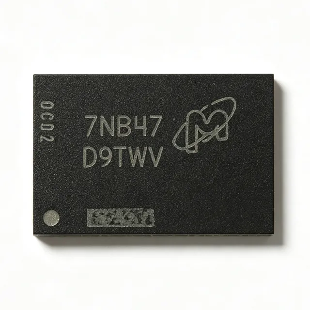
MT40A256M16GE-075E:B - 4Gb DDR4 SDRAM 2666 MT/s | Micron
MPN: MT40A256M16GE-075E:B ✓ 啟用中| 數量 | 單價 | 小計 |
|---|---|---|
| 1 | $5.15 | $5.15 |
| 10 | $4.89 | $48.90 |
| 100 | $4.55 | $455.00 |
| 500 | $4.25 | $2,125.00 |
| 1,000 | $3.95 | $3,950.00 |
MT40A256M16GE-075E:B 概覽
DDR4 SDRAM (Double Data Rate 4 Synchronous Dynamic Random Access Memory) is the fourth generation of the DDR DRAM family, sitting within the hierarchy: DRAM -> SDRAM -> DDR SDRAM -> DDR4 -> volatile memory IC. DDR4 doubles the bank count and lowers the operating voltage relative to DDR3, improving bandwidth and power efficiency in computing, networking, and embedded systems. The JEDEC-defined DDR4 interface uses a pseudo open-drain I/O at 1.2V, along with on-die termination and adjustable internal VREFDQ generation to maintain signal integrity at high data rates.
Key features of this device include 16 internal banks, temperature-controlled refresh (TCR) that extends refresh interval automatically up to 95C, and both 64ms/8192-cycle refresh (at <=85C per JEDEC convention) and 32ms/8192-cycle refresh modes. The 1.2V pseudo open-drain I/O reduces I/O power compared to DDR3L, and on-die internal adjustable VREFDQ generation eliminates the need for external reference voltage routing on the PCB.
Architecturally, the die uses 256Mbit x16 organization with DDR4's bank-group structure, supporting burst lengths of 8 with sequential and interleaved options, and commands are registered on both clock edges to achieve the 2666 MT/s rate. VPP core supply is 2.5V (-125mV/+250mV) per Micron datasheet documentation.
Typical applications include FPGA and processor memory subsystems (such as AMD Zynq UltraScale+ MPSoC designs), networking line cards, industrial controllers, and embedded computing modules requiring a 16-bit-wide DDR4 interface.
Design consideration: verify the memory controller's supported speed grades and the -075E (2666 MT/s) timing set against your clock plan; derate to DDR4-2133 or DDR4-2400 operating points if board topology limits signal integrity.
This page synthesizes distributor pricing, drop-in same-package alternatives, lifecycle notes, and practical design guidance not found in the manufacturer datasheet. Price references are as of 2026-09-03.
直接替換替代品,適用於 MT40A256M16GE-075E:B — 相同封裝,腳位對腳位相容。需重新設計 PCB 的不同封裝零件不列入。
此系列的變體
與下列產品可直接替換的同系列型號: MT40A256M16GE-075E:B (相同外形與佔位) — 差異在於 Package, Interface, Data Rate, RoHS Status, Organization.
快速比較工具 — 選擇替代零件進行並排比較:
MT40A256M16GE-075E IT:B
📋 參考替代品(不在目錄中)
MT40A256M16GE-075E:AUT:B
📋 參考替代品(不在目錄中)
MT40A256M16GE-075E:AAT:B
📋 參考替代品(不在目錄中)
MT40A256M16GE-083E:B
📋 參考替代品(不在目錄中)
MT40A256M16GE-062E:B
📋 參考替代品(不在目錄中)
MT40A256M16GE-075E:B 最大額定值與電氣特性
| 記憶體類型 | DDR4 SDRAM |
| 記憶體容量 | 4 Gbit |
| 組織 | 256M x 16 |
| Memory Interface | Parallel |
| Clock Frequency | 1.33 GHz |
| 資料速率 | 2666 MT/s (DDR4-2666) |
| VDD / VDDQ | 1.2 V +/-60 mV |
| VPP | 2.5 V, -125 mV/+250 mV |
| Internal Banks | 16 |
| Refresh | 64 ms / 8192-cycle; 32 ms / 8192-cycle at 95C |
| I/O Type | 1.2 V pseudo open-drain |
| VREFDQ | On-die, internal, adjustable generation |
| Special Features | Temperature controlled refresh (TCR) |
| 封裝 | 96-FBGA (9 x 14 mm) |
| 安裝類型 | Surface Mount |
MT40A256M16GE-075E:B 96-fbga (9 x 14 mm) 腳位配置指南
MT40A256M16GE-075E:B(96-fbga (9 x 14 mm) 封裝)的腳位配置。 此數位 IC 包含 GPIO、通訊介面(UART、SPI、I2C)與電源腳位。替代腳位功能與配置選項請參閱製造商資料表。對嵌入式系統設計與 PCB 佈局至關重要。

無詳細腳位定義資料: MT40A256M16GE-075E:B.
請參閱 資料表 以查看完整腳位配置。
典型應用
MT40A256M16GE-075E:B 適用於 6 應用s: FPGA / Zynq UltraScale+ MPSoC Memory, Networking Line Cards and Switches, Industrial Control and Automation, Automotive Infotainment and ADAS, Embedded Computing Modules (SoM/COM Express), Test and Measurement Instrumentation.
FPGA / Zynq UltraScale+ MPSoC Memory
The MT40A256M16GE-075E:B fits FPGA and MPSoC memory subsystems such as AMD Zynq UltraScale+ (ZU4CG) designs, where its DDR4-2666 rating provides timing margin above the 1200 MHz DDR controller clock and its x16 organization enables easy 32-bit and 64-bit bus scaling with two or four devices. In Vivado MIG-based designs, the on-die adjustable VREFDQ removes external reference routing, simplifying escape routing under dense BGA fanout. The -075E grade gives setup/hold margin at slightly derated operating points, which is valuable on 6-8 layer boards where fly-by routing cannot always achieve full DDR4-2666 eye margins. Because the family is obsolete, use it for sustaining existing designs and migrate new designs to current-production DDR4.
推薦
Networking Line Cards and Switches
Enterprise switches and router line cards use x16 DDR4 devices for packet buffer and lookup table memory, and the MT40A256M16GE-075E:B's 2666 MT/s rate and 16 internal banks deliver the bandwidth and low effective row-conflict latency these datapaths require. The 1.2V pseudo open-drain I/O lowers I/O switching power versus DDR3L, reducing thermal load on densely populated line cards. Temperature-controlled refresh adapts refresh rates to the card's internal ambient, cutting refresh power overhead by up to 50% in cool-aisle conditions. Four devices on a 64-bit bus provide 8 GB-class buffer memory at moderate cost, and the 96-FBGA footprint keeps height low for front-access card guides.
推薦
Industrial Control and Automation
Programmable logic controllers, motion controllers, and machine-vision systems require dependable working memory across wide temperature ranges. The MT40A256M16GE-075E IT:B variant is specified from -40C to +95C, covering sealed cabinet environments where ambient can exceed 70C. Its 4Gb density supports Linux-based soft controllers with file caching, while the x16 bus keeps DRAM controller complexity and power low. On-die VREFDQ generation improves noise immunity against motor-drive switching noise coupled into memory nets. The temperature-controlled refresh feature reduces refresh current at lower cabinet temperatures, saving power in battery-buffered systems. Design with the IT variant and verify controller timing at the derated operating point for long-term margin.
推薦
Automotive Infotainment and ADAS
Automotive infotainment head units and ADAS perception ECUs need DDR4 with AEC-Q100 qualification for cabin and near-engine environments. The MT40A256M16GE-075E:AUT:B provides that qualification in the identical 96-FBGA footprint, easing reuse of validated PCB layouts across carline platforms. The DDR4-2666 rate supports multi-camera ADAS pipelines and HD graphics frame buffers, while the 1.2V interface reduces power dissipation inside thermally constrained dashboard enclosures. Designers should verify the memory controller's automotive timing tables against the -075E speed bin and confirm supply continuity with Flip Electronics given the family's obsolete catalog status. Temperature-controlled refresh helps maintain bandwidth consistency across -40C cold crank to 95C soak conditions.
推薦
Embedded Computing Modules (SoM/COM Express)
System-on-module and COM Express carriers populate x16 DDR4 components on both module sides to reach 2-8 GB densities in minimal board area. The MT40A256M16GE-075E:B's 9 x 14 mm 96-FBGA package and 1.2V signaling are well matched to this construction: the BGA balls provide reliable second-level interconnect under thermal cycling, and the low I/O voltage limits per-net switching current when stacks of eight devices share address/command nets in fly-by topology with on-die termination. The 2666 MT/s grade gives margin for the length-matched top/bottom routing typical of modules. For modules sold into industrial and transportation markets, select the IT temperature variant to meet -40C cold-start requirements.
推薦
Test and Measurement Instrumentation
Oscilloscopes, logic analyzers, and arbitrary waveform generators rely on deep capture memory; x16 DDR4 parts like the MT40A256M16GE-075E:B supply 4Gb per device, allowing 8 GB of record length with sixteen components. The 16-bank architecture reduces effective random-access latency when the acquisition engine streams data to memory, and DDR4-2666 sustains the sustained write bandwidth needed for multi-channel, high-sample-rate capture. On-die VREFDQ keeps the reference plane clean on boards crowded with high-speed analog front-end circuitry. Instrument vendors should note the obsolescence of this speed bin and qualify a current-production replacement before the next service-life refresh cycle.
推薦
推薦產品摘要
工程參考資料,適用於 MT40A256M16GE-075E:B — 比較、設計指引及合規資訊。
選型指南
與替代品比較
| 參數 | 本產品 | MT40A256M16GE-075E IT | MT40A256M16GE-075E | MT40A256M16GE-083E | MT40A256M16GE-062E |
|---|---|---|---|---|---|
| Package | 96-FBGA (9 x 14 mm) | B: 96-FBGA (9 x 14 mm) - same | AUT:B: 96-FBGA (9 x 14 mm) - same | B: 96-FBGA (9 x 14 mm) - same | B: 96-FBGA (9 x 14 mm) - same |
| Brand | Micron Technology | B: Micron Technology | AUT:B: Micron Technology | B: Micron Technology | B: Micron Technology |
| Density / Organization | 4 Gbit, 256M x 16 | B: 4 Gbit, 256M x 16 | AUT:B: 4 Gbit, 256M x 16 | B: 4 Gbit, 256M x 16 | B: 4 Gbit, 256M x 16 |
| Data Rate | 2666 MT/s (DDR4-2666) | B: 2666 MT/s | AUT:B: 2666 MT/s | B: 2400 MT/s | B: 3200 MT/s |
| VDD / VDDQ | 1.2 V +/-60 mV | B: 1.2 V +/-60 mV | AUT:B: 1.2 V +/-60 mV | B: 1.2 V +/-60 mV | B: 1.2 V +/-60 mV |
| Internal Banks | 16 | B: 16 | AUT:B: 16 | B: 16 | B: 16 |
主要差異化特點
- Highest speed grade within the same family footprint (對比MT40A256M16GE-083E:B)
- Industrial temperature option available in the same footprint (對比MT40A256M16GE-075E IT:B)
- AEC-Q100 automotive qualification path (對比MT40A256M16GE-075E:AUT:B)
設計說明
For DDR4-2666 operation, follow the Micron datasheet PCB design guide: fly-by address/command routing with on-die termination, length-matched data groups within +/-25 mil per 1000 mil of trace, and a solid reference plane under every memory net. The on-die adjustable VREFDQ removes the external reference voltage net, but keep DQ/DM/DQS pairs tightly coupled to their own return path. On 6-layer boards, derate to DDR4-2400 if eye-margin testing at the -075E bin shows closure at temperature extremes.
Budget the 1.2V VDD/VDDQ rail for the full DDR4-2666 active current plus refresh, and supply VPP at 2.5V (-125mV/+250mV) per the datasheet; VPP back-biasing of the cell array means its current is small but rail accuracy still matters. Enable temperature-controlled refresh (TCR) in the controller so refresh rate relaxes below 85C, cutting refresh power measurably in typical ambient conditions. Estimated: at moderate utilization a single x16 device typically draws several hundred milliamps on the 1.2V rail - verify with Micron's current DDR4 power calculator for your exact usage model.
The -075E suffix is a speed bin, not a temperature code - do not assume the base part covers -40C; specify the IT variant for industrial ranges. Second, this whole MT40A256M16GE family appears in Micron's obsolete catalog, so design-in without a second source or last-time-buy plan is risky: AMD community threads already report shortages for Zynq-based designs. Finally, when substituting -083E for -075E, update the memory controller timing table - the footprint is identical but DDR4-2400 settings are required for guaranteed operation.
合規資訊
RoHS compliance per distributor listing (B suffix denotes RoHS/lead-free packaging). AEC-Q100 applies only to the AUT variants (MT40A256M16GE-075E:AUT:B / AAT:B). REACH and halogen-free status not stated in provided data.





