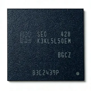
K3KLELE0DM-BGCU - 144Gb LPDDR5X 8533Mbps DRAM | Samsung
料号: K3KLELE0DM-BGCU ✗ 停产| 数量 | 单价 | 小计 |
|---|---|---|
| 1 | $0 | $0.00 |
| 10 | $0 | $0.00 |
| 100 | $0 | $0.00 |
| 500 | $0 | $0.00 |
| 1,000 | $0 | $0.00 |
K3KLELE0DM-BGCU 概述
LPDDR5X is the premium tier of the low-power DRAM family, which sits within the broader DRAM -> volatile memory -> semiconductor memory hierarchy. Unlike DDR5 server DRAM, LPDDR5X is architected for bandwidth-per-watt: it attaches directly to the host SoC in a point-to-point topology on the same PCB, eliminating DIMM connectors and reducing trace length and load.
Key features include the 144 Gb density (18 GB equivalent when used in x64 organization per die stack), the 8533 Mbps pin speed, which Samsung states is approximately 1.25 times faster than the previous LPDDR generation, and about 25% better power efficiency enabled by lower core voltage and advanced I/O calibration. The multi-voltage architecture separates core (0.5 V region), I/O and interface rails for fine-grained power management.
Technically, LPDDR5X uses sophisticated training, DFE (decision feedback equalization) on reads, and per-byte write CRC to sustain 8533 Mbps signaling integrity. Bank-group and deep-bank organization reduce row-conflict latency for AI workloads.
Typical applications include AI accelerators and edge AI modules, premium smartphones and tablets, automotive infotainment and ADAS platforms, and high-performance embedded computing where memory bandwidth per watt is the limiting factor.
Design consideration: the part is marked EOL by the source listing, so new designs should plan lifecycle management or dual-source qualification; verify availability before committing to production.
This page synthesizes distributor stock listings, spec aggregation, and drop-in alternatives not found in a single manufacturer datasheet.
直接替换替代料: K3KLELE0DM-BGCU ——相同封装,引脚兼容。需要 PCB 改动的不同封装料号已排除。
本系列中的变体
可与以下型号直接替换的同系列型号: K3KLELE0DM-BGCU (相同外形与封装尺寸) ——差异在于 Density, Interface, Package, Memory Type, Mounting Type.
快速对比工具——选择替代料号进行并排对比:
K3KL5L50DM-BGCU
✅ 直接替换 ⚠️ 规格未核验✓ 有现货
联系询价
查看数据手册 →K3KL3L30DM-BGCU
✅ 直接替换 ⚠️ 规格未核验✓ 有现货
$45.9375 / 个
查看数据手册 →K3KLALA0DM-MGCU
✅ 直接替换 ⚠️ 规格未核验✓ 有现货
联系询价
查看数据手册 →K3KL9L90DM-JGCT
✅ 直接替换 ⚠️ 规格未核验✓ 有现货
$65.18 / 个
查看数据手册 →K3KL8L80DM-MGCU
✅ 直接替换 ⚠️ 规格未核验✓ 有现货
联系询价
查看数据手册 →K3KL4L40EM-BGCU
✅ 直接替换 ⚠️ 规格未核验✓ 有现货
$78.75 / 个
查看数据手册 →K3KLELE0DM-BGCU 最大额定值与电气特性
| Density | 144 Gb |
| 存储器类型 | LPDDR5X SDRAM |
| 存储组织 | x64 |
| 数据速率 | 8533 Mbps |
| Supply Voltage (VDD1) | 1.8 V |
| Supply Voltage (VDD2) | 1.05 V |
| Supply Voltage (VDDQ) | 0.9 V |
| Supply Voltage (VDDCA) | 0.5 V |
| 封装 | 496-ball FBGA |
| 工作温度 | -25 C to +85 C |
| 安装类型 | Surface Mount |
| Application Class | AI and in-vehicle devices |
| Product Status | EOL |
| 接口 | LPDDR5X |
| Power Efficiency vs Previous Generation | Approx. 25% better (per Samsung) |
| Speed vs Previous Generation | Approx. 1.25x faster (per Samsung) |
K3KLELE0DM-BGCU 496-ball fbga 引脚配置指南
K3KLELE0DM-BGCU(496-ball fbga 封装)的引脚配置。 该数字 IC 包含 GPIO、通信接口(UART、SPI、I2C)和电源引脚。请参阅制造商数据手册以了解复用引脚功能和配置选项。对嵌入式系统设计和 PCB 布局至关重要。

暂无详细引脚数据: K3KLELE0DM-BGCU.
请参阅 数据手册 以查看完整引脚配置。
典型应用
K3KLELE0DM-BGCU 适用于 6 应用s: AI Edge Accelerators, Automotive Infotainment and ADAS, Premium Smartphones and Tablets, High-Performance Embedded Computing, Networking and Edge Servers, Data Center Accelerator Memory (PCB-Attach).
AI Edge Accelerators
The K3KLELE0DM-BGCU provides 144 Gb of local memory with 8533 Mbps bandwidth, directly addressing the memory-bandwidth bottleneck of edge AI inference. With an x64 organization and LPDDR5X signaling, the device sustains high read throughput for transformer and CNN workloads while Samsung's stated ~25% power-efficiency gain versus the previous generation reduces thermal load in fanless enclosures. Placed point-to-point next to the AI SoC on the same PCB, the 496-ball FBGA minimizes trace length, improving signal integrity at 8533 Mbps. The multi-rail supply (1.8/1.05/0.9/0.5 V) allows the host PMIC to scale voltage with workload, trading peak performance for idle power.
推荐
Automotive Infotainment and ADAS
The device's -25 to +85 C operating range covers automotive cabin environments, and Samsung explicitly targets in-vehicle devices with this LPDDR5X class. Instrument clusters, infotainment SoCs and ADAS perception units require both high display-refresh bandwidth and low latency; the 8533 Mbps rate and LPDDR5X write CRC support error-robust operation. In the 496-ball FBGA footprint, the memory attaches directly to the automotive SoC, avoiding DIMM connectors that suffer vibration reliability issues. Designers should confirm the exact ordering code's automotive qualification level and, given the EOL status, align last-time-buy quantities with the vehicle program's service life.
推荐
Premium Smartphones and Tablets
LPDDR5X was developed to transcend mobile devices, per Samsung, and this 144 Gb (18 GB-class) package suits flagship smartphones and tablets needing large app footprints, high-resolution cameras and on-device AI. The roughly 1.25x speed increase and 25% efficiency gain versus the previous generation translate directly into faster memory copies and longer battery life. The point-to-point 496 FBGA attach keeps the PCB footprint minimal inside thin form factors. Note that the EOL status makes this MPN primarily a service/repair and short-run sourcing item for mobile platforms; new flagship designs should adopt Samsung's successor LPDDR5X ordering codes.
推荐
High-Performance Embedded Computing
Embedded compute modules (COMs, SOMs) used in test, vision and industrial robotics benefit from the 144 Gb density and 8533 Mbps bandwidth per package, enabling large frame buffers and data-logging caches without switching to power-hungry DDR5 server memory. LPDDR5X's multi-rail power architecture (1.8/1.05/0.9/0.5 V) integrates cleanly with standard LPDDR PMICs, and the -25 to +85 C range suits industrial enclosures. At 8533 Mbps, layout rules are strict: matched-length fly-by-less point-to-point routing and solid reference planes are mandatory. The EOL status warrants early lifetime planning for multi-year industrial programs.
推荐
Networking and Edge Servers
Edge servers, 5G baseband units and network appliances need substantial memory bandwidth under constrained power budgets. The K3KLELE0DM-BGCU's 8533 Mbps rate provides the per-package bandwidth for packet buffering, TLS offload and on-box inference, while LPDDR5X efficiency helps meet the telecom power-envelope targets. The 496-ball FBGA is directly compatible with memory subsystems of embedded network SoCs supporting LPDDR5X. Because the part is EOL, network equipment makers should treat current broker stock (Wolfchip reported 39,600 pcs as of Aug 05, 2026) as finite and qualify a successor Samsung LPDDR5X code for future builds.
推荐
Data Center Accelerator Memory (PCB-Attach)
For accelerator cards that use PCB-attached LPDDR5X as a capacity tier beside HBM, the 144 Gb K3KLELE0DM-BGCU offers high per-package density; multiple packages can be grouped to reach tens of GB of scratch memory for recommendation models and LLM KV-caches. The 8533 Mbps rate with decision-feedback equalization maintains eye margins on controlled-impedance PCB traces up to the lengths defined in the LPDDR5X spec class, while the 0.5 V interface rail keeps I/O power low at scale. Rack thermal designs must account for the -25 to +85 C operating window and package power during sustained training bursts.
推荐
推荐产品汇总
工程参考数据: K3KLELE0DM-BGCU ——对比、设计指导和合规信息。
选型指南
与替代料对比
| 参数 | 本产品 | K3KL5L50DM-BGCU | K3KL3L30DM-BGCU | K3KLALA0DM-MGCU | K3KL9L90DM-JGCT |
|---|---|---|---|---|---|
| Package | 496-ball FBGA | 496-ball FBGA - same | 496-ball FBGA - same | 496-ball FBGA - same | 496-ball FBGA - same |
| Brand | Samsung Electronics | Samsung Electronics | Samsung Electronics | Samsung Electronics | Samsung Electronics |
| Interface | LPDDR5X | LPDDR5X | LPDDR5X | LPDDR5X | LPDDR5X |
| Organization | x64 | x64 | x64 | x64 | x64 |
关键差异点
- Maximum density in footprint (对比 K3KL5L50DM-BGCU)
- Top LPDDR5X speed bin (对比 K3KLALA0DM-MGCU)
- Power efficiency for thermal-limited systems (对比 K3KL9L90DM-JGCT)
设计说明
At 8533 Mbps, LPDDR5X routing requires strict matched-length, point-to-point traces between the SoC and K3KLELE0DM-BGCU with controlled impedance (typically 40-50 ohm single-ended per the controller design guide). Avoid stubs, minimize layer transitions, and maintain solid reference planes under all DQ/CA/DQS nets. Read DFE and write CRC help at the receiver but cannot compensate for gross length mismatch - follow the SoC vendor's LPDDR5X layout checklist before tape-out.
Design a four-rail power tree: 1.8 V (VDD1), 1.05 V (VDD2), 0.9 V (VDDQ) and 0.5 V (interface rail), per the verified spec data. Use a PMIC with LPDDR5X mode to sequence rails and to support VDD2 core-voltage scaling, which is the source of the ~25% efficiency gain Samsung cites versus the previous generation. Estimated: peak package current scales with density and speed, so size regulators using your controller's power spreadsheet, not nominal rail voltage alone.
The part is EOL per distributor data, so a design that qualifies only this MPN faces supply risk within the product's service life. Recommended: (1) confirm stock and date codes with the distributor before design freeze, (2) place a last-time-buy covering the full program lifetime, and (3) pre-qualify a Samsung successor LPDDR5X ordering code in the same 496-ball FBGA footprint to allow drop-in migration without PCB respin.
合规信息
No compliance data appears in the verified web data for this MPN. Samsung memory products are generally RoHS-compliant, but this must be confirmed on the official Samsung product page before use in regulated markets.