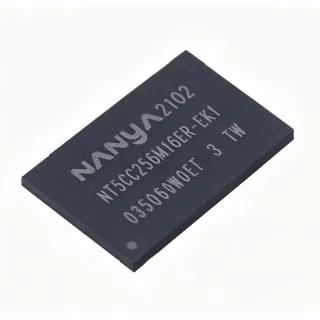
NT5CC256M16CP-EK - 4Gb DDR3L SDRAM 256Mx16 | Nanya Technology
料号: NT5CC256M16CP-EK ✓ 量产中| 数量 | 单价 | 小计 |
|---|---|---|
| 1 | $30.12 | $30.12 |
| 10 | $28.5 | $285.00 |
| 100 | $26 | $2,600.00 |
| 500 | $24 | $12,000.00 |
| 1,000 | $22 | $22,000.00 |
NT5CC256M16CP-EK 概述
DDR3L (Double Data Rate 3 Low Voltage) SDRAM is a type of synchronous dynamic random-access memory that operates at a lower voltage (1.35V) compared to standard DDR3 (1.5V), reducing power consumption by up to 20% while maintaining similar performance. It is part of the DRAM memory hierarchy, which includes SRAM, DRAM, and flash memory, and is widely used in main memory, graphics, and embedded applications.
Key features include a 4Gb density, 256M x 16 organization, 96-ball TFBGA package, and support for both DDR3 and DDR3L operation. The device operates over a temperature range of 0°C to +95°C (TC) and includes features such as auto self-refresh, auto precharge, asynchronous reset, data mask, write leveling, dynamic on-chip termination, and ZQ calibration. These features enhance signal integrity and system reliability.
The NT5CC256M16CP-EK uses an 8n-prefetch architecture with 8 internal memory banks, differential clock inputs (CK, CK#), and programmable CAS latency (CL), write latency (CWL), and additive latency. It supports burst lengths of 8 and 4 with burst chop, and includes on-die termination (ODT) for improved signal quality. The device is RoHS compliant and lead-free.
Typical applications include servers, networking equipment, industrial computing, automotive infotainment, and consumer electronics such as set-top boxes and smart TVs. Its low-voltage operation makes it ideal for power-sensitive designs, while its high-speed interface supports demanding data-intensive workloads.
When designing with this device, ensure proper decoupling capacitors near the power pins and follow the layout guidelines in the datasheet to minimize signal integrity issues. The ZQ calibration pin requires a 240-ohm resistor to ground for proper impedance calibration.
直接替换替代料: NT5CC256M16CP-EK ——相同封装,引脚兼容。需要 PCB 改动的不同封装料号已排除。
本系列中的变体
可与以下型号直接替换的同系列型号: NT5CC256M16CP-EK (相同外形与封装尺寸) ——差异在于 Package, Supply Voltage, Data Rate, Density, Operating Temperature.
快速对比工具——选择替代料号进行并排对比:
NT5CC256M16ER-EK
✅ 直接替换✓ 有现货
$24 / 个
查看数据手册 →NT5CC256M16DP-EK
✅ 直接替换 ⚠️ 规格未核验📋 参考替代料(不在目录中)
NT5CC256M16EP-EK
✅ 直接替换 ⚠️ 规格未核验📋 参考替代料(不在目录中)
MT41K256M16HA-125
✅ 直接替换 ⚠️ 规格未核验✓ 有现货
$6.3636 / 个
查看数据手册 →K4B4G1646E-BYMA
✅ 直接替换 ⚠️ 规格未核验✓ 有现货
$14.3182 / 个
查看数据手册 →NT5CC256M16CP-EK 最大额定值与电气特性
| 存储器类型 | DDR3L SDRAM |
| Density | 4Gb |
| 存储组织 | 256M x 16 |
| 电源电压 | 1.35V (DDR3L) / 1.5V (DDR3) |
| 数据速率 | 2133 Mb/s per pin |
| 封装 | 96-ball TFBGA |
| 工作温度 | 0°C to +95°C (TC) |
| Number of Banks | 8 |
| Refresh Cycles | 8192 |
| CAS Latency (CL) | Programmable (e.g., 9, 10, 11, 12, 13) |
| Write Latency (CWL) | 5, 6, 7, 8, 9 |
| Burst Length | 8 and 4 (with burst chop) |
| 接口 | Differential clock (CK, CK#) |
| RoHS | Compliant |
| Lead-Free | Yes |
NT5CC256M16CP-EK 引脚配置
| 引脚 A1 | VDD — Power supply (1.35V/1.5V) |
| 引脚 A2 | DQ0 — Data input/output 0 |
| 引脚 A3 | DQ1 — Data input/output 1 |
| 引脚 A4 | VSS — Ground |
| 引脚 A5 | DQ2 — Data input/output 2 |
| 引脚 A6 | DQ3 — Data input/output 3 |
| 引脚 A7 | VDD — Power supply |
| 引脚 A8 | DQ4 — Data input/output 4 |
| 引脚 A9 | DQ5 — Data input/output 5 |
| 引脚 A10 | VSS — Ground |
| 引脚 A11 | DQ6 — Data input/output 6 |
| 引脚 A12 | DQ7 — Data input/output 7 |
| 引脚 B1 | VSS — Ground |
| 引脚 B2 | DQ8 — Data input/output 8 |
| 引脚 B3 | DQ9 — Data input/output 9 |
| 引脚 B4 | VDD — Power supply |
| 引脚 B5 | DQ10 — Data input/output 10 |
| 引脚 B6 | DQ11 — Data input/output 11 |
| 引脚 B7 | VSS — Ground |
| 引脚 B8 | DQ12 — Data input/output 12 |
| 引脚 B9 | DQ13 — Data input/output 13 |
| 引脚 B10 | VDD — Power supply |
| 引脚 B11 | DQ14 — Data input/output 14 |
| 引脚 B12 | DQ15 — Data input/output 15 |
| 引脚 C1 | VDDQ — DQ power supply |
| 引脚 C2 | VSSQ — DQ ground |
| 引脚 C3 | VDDQ — DQ power supply |
| 引脚 C4 | VSSQ — DQ ground |
| 引脚 C5 | VDDQ — DQ power supply |
| 引脚 C6 | VSSQ — DQ ground |
| 引脚 C7 | VDDQ — DQ power supply |
| 引脚 C8 | VSSQ — DQ ground |
| 引脚 C9 | VDDQ — DQ power supply |
| 引脚 C10 | VSSQ — DQ ground |
| 引脚 C11 | VDDQ — DQ power supply |
| 引脚 C12 | VSSQ — DQ ground |
| 引脚 D1 | A0 — Address input 0 |
| 引脚 D2 | A1 — Address input 1 |
| 引脚 D3 | A2 — Address input 2 |
| 引脚 D4 | A3 — Address input 3 |
| 引脚 D5 | A4 — Address input 4 |
| 引脚 D6 | A5 — Address input 5 |
| 引脚 D7 | A6 — Address input 6 |
| 引脚 D8 | A7 — Address input 7 |
| 引脚 D9 | A8 — Address input 8 |
| 引脚 D10 | A9 — Address input 9 |
| 引脚 D11 | A10/AP — Address input 10 / Auto-precharge |
| 引脚 D12 | A11 — Address input 11 |
| 引脚 E1 | A12 — Address input 12 |
| 引脚 E2 | A13 — Address input 13 |
| 引脚 E3 | A14 — Address input 14 |
| 引脚 E4 | A15 — Address input 15 |
| 引脚 E5 | BA0 — Bank address 0 |
| 引脚 E6 | BA1 — Bank address 1 |
| 引脚 E7 | BA2 — Bank address 2 |
| 引脚 E8 | RAS# — Row address strobe |
| 引脚 E9 | CAS# — Column address strobe |
| 引脚 E10 | WE# — Write enable |
| 引脚 E11 | CS# — Chip select |
| 引脚 E12 | CKE — Clock enable |
| 引脚 F1 | ODT — On-die termination |
| 引脚 F2 | CK — Clock (positive) |
| 引脚 F3 | CK# — Clock (negative) |
| 引脚 F4 | VDD — Power supply |
| 引脚 F5 | VSS — Ground |
| 引脚 F6 | VDD — Power supply |
| 引脚 F7 | VSS — Ground |
| 引脚 F8 | VDD — Power supply |
| 引脚 F9 | VSS — Ground |
| 引脚 F10 | VDD — Power supply |
| 引脚 F11 | VSS — Ground |
| 引脚 F12 | VDD — Power supply |
| 引脚 G1 | DM0 — Data mask 0 |
| 引脚 G2 | DM1 — Data mask 1 |
| 引脚 G3 | DM2 — Data mask 2 |
| 引脚 G4 | DM3 — Data mask 3 |
| 引脚 G5 | VSS — Ground |
| 引脚 G6 | VDD — Power supply |
| 引脚 G7 | VSS — Ground |
| 引脚 G8 | VDD — Power supply |
| 引脚 G9 | VSS — Ground |
| 引脚 G10 | VDD — Power supply |
| 引脚 G11 | VSS — Ground |
| 引脚 G12 | VDD — Power supply |
| 引脚 H1 | DQS0 — Data strobe 0 (positive) |
| 引脚 H2 | DQS0# — Data strobe 0 (negative) |
| 引脚 H3 | DQS1 — Data strobe 1 (positive) |
| 引脚 H4 | DQS1# — Data strobe 1 (negative) |
| 引脚 H5 | DQS2 — Data strobe 2 (positive) |
| 引脚 H6 | DQS2# — Data strobe 2 (negative) |
| 引脚 H7 | DQS3 — Data strobe 3 (positive) |
| 引脚 H8 | DQS3# — Data strobe 3 (negative) |
| 引脚 H9 | VSS — Ground |
| 引脚 H10 | VDD — Power supply |
| 引脚 H11 | VSS — Ground |
| 引脚 H12 | VDD — Power supply |
| 引脚 J1 | RESET# — Asynchronous reset |
| 引脚 J2 | TDQS — Termination data strobe |
| 引脚 J3 | TDQS# — Termination data strobe (negative) |
| 引脚 J4 | ZQ — ZQ calibration |
| 引脚 J5 | VDD — Power supply |
| 引脚 J6 | VSS — Ground |
| 引脚 J7 | VDD — Power supply |
| 引脚 J8 | VSS — Ground |
| 引脚 J9 | VDD — Power supply |
| 引脚 J10 | VSS — Ground |
| 引脚 J11 | VDD — Power supply |
| 引脚 J12 | VSS — Ground |
典型应用
NT5CC256M16CP-EK 适用于 6 应用s: Server Memory, Networking Equipment, Industrial Computing, Automotive Infotainment, Consumer Electronics, Embedded Systems.
Server Memory
The NT5CC256M16CP-EK provides high-density, low-power memory for server applications. Its 4Gb density and 2133 Mb/s data rate support demanding workloads, while DDR3L operation reduces power consumption in data centers. The 96-ball TFBGA package enables compact module designs, and features like ECC support (if available) enhance reliability. When used in registered DIMMs, it pairs with a register clock driver (RCD) to buffer address and control signals, ensuring signal integrity at high speeds. The low voltage also reduces thermal load, improving system cooling efficiency.
推荐
Networking Equipment
In networking equipment such as routers and switches, the NT5CC256M16CP-EK provides fast, low-power memory for packet buffering and routing tables. Its high data rate (2133 Mb/s) ensures low latency, while DDR3L voltage reduces power in always-on network devices. The device's on-die termination (ODT) and write leveling features improve signal integrity on high-speed buses, critical for reliable data transmission. It can be used in conjunction with a network processor or FPGA to handle data plane tasks. The 96-ball TFBGA package allows for dense PCB layouts, saving board space in compact networking hardware.
推荐
Industrial Computing
The NT5CC256M16CP-EK is suitable for industrial PCs and embedded systems that require reliable operation over extended temperature ranges (0°C to +95°C). Its low power consumption is beneficial for fanless designs, and the high data rate supports real-time data processing. The device's auto self-refresh and ZQ calibration features ensure stable operation in varying thermal conditions. It can be paired with an industrial-grade processor or FPGA for applications like machine vision and process control. The 96-ball TFBGA package provides robust solder joints for vibration-prone environments.
推荐
Automotive Infotainment
In automotive infotainment systems, the NT5CC256M16CP-EK provides high-bandwidth memory for navigation, multimedia, and instrument cluster displays. Its DDR3L operation reduces power consumption, which is critical in vehicles. The device supports a wide temperature range, making it suitable for cabin environments. Features like write leveling and dynamic ODT ensure reliable operation in noisy automotive electrical environments. It can be used with an automotive-grade application processor or SoC. The 96-ball TFBGA package is compact, fitting into space-constrained head units.
推荐
Consumer Electronics
The NT5CC256M16CP-EK is used in consumer devices like set-top boxes, smart TVs, and gaming consoles. Its high data rate enables smooth video streaming and responsive user interfaces, while DDR3L voltage reduces power consumption in always-on devices. The device's small TFBGA package allows for slim product designs. It can be paired with a media processor or SoC for video decoding and rendering. Features like auto precharge and burst chop improve memory efficiency, reducing latency in real-time applications.
推荐
Embedded Systems
For general embedded systems, the NT5CC256M16CP-EK offers a balance of performance and power efficiency. Its 4Gb density is suitable for applications requiring large memory footprints, such as data logging and complex algorithms. The device's low voltage and wide temperature range make it versatile for various environments. It can be interfaced with a wide range of microcontrollers and FPGAs that support DDR3L. The 96-ball TFBGA package is easy to route on multi-layer PCBs. Features like on-die termination simplify PCB design by reducing the need for external termination resistors.
推荐
推荐产品汇总
工程参考数据: NT5CC256M16CP-EK ——对比、设计指导和合规信息。
选型指南
与替代料对比
| 参数 | 本产品 | NT5CC256M16ER-EK | NT5CC256M16DP-EK | MT41K256M16HA-125 |
|---|---|---|---|---|
| Package | 96-ball TFBGA | 96-ball TFBGA | 96-ball TFBGA | 96-ball FBGA |
| Brand | Nanya Technology | Nanya Technology | Nanya Technology | Micron Technology |
| Density | 4Gb | 4Gb | 4Gb | 4Gb |
| Organization | 256M x 16 | 256M x 16 | 256M x 16 | 256M x 16 |
| Supply Voltage | 1.35V (DDR3L) | 1.35V (DDR3L) | 1.35V (DDR3L) | 1.35V (DDR3L) |
| Data Rate | 2133 Mb/s | 2133 Mb/s | 2133 Mb/s | 2133 Mb/s |
| Operating Temperature | 0°C to +95°C | 0°C to +95°C | 0°C to +95°C | 0°C to +95°C |
| Number of Banks | 8 | 8 | 8 | 8 |
关键差异点
- Low-voltage DDR3L operation (对比 Standard DDR3 parts)
- Wide temperature range (对比 Commercial-only DDR3L parts)
- High data rate (对比 Older DDR3L parts with lower speed grades)
设计说明
For high-speed DDR3L signals, maintain controlled impedance of 40-60 ohms for data lines and 50-75 ohms for address/control lines. Keep trace lengths matched within +/- 50 mils for DQ/DQS groups. Use a solid ground plane beneath the memory device and minimize vias on high-speed traces. Refer to the Nanya layout guidelines in the datasheet for specific recommendations.
Decouple VDD and VDDQ with 0.1uF and 1uF ceramic capacitors placed as close to the balls as possible. Use a 10uF bulk capacitor per power rail. The ZQ pin requires a 240-ohm +/- 1% resistor to ground for impedance calibration. Ensure the VREF voltage is clean and properly bypassed.
The NT5CC256M16CP-EK operates up to +95°C TC. For high-density systems, ensure adequate airflow or heatsinking to keep the case temperature within limits. The 96-ball TFBGA package has a thermal resistance that depends on PCB copper area; use thermal vias under the package to improve heat dissipation.
合规信息
RoHS compliant and lead-free per datasheet and distributor listings. AEC-Q100 not specified for this part number; automotive grade may require specific suffix.