Products (39,000+)

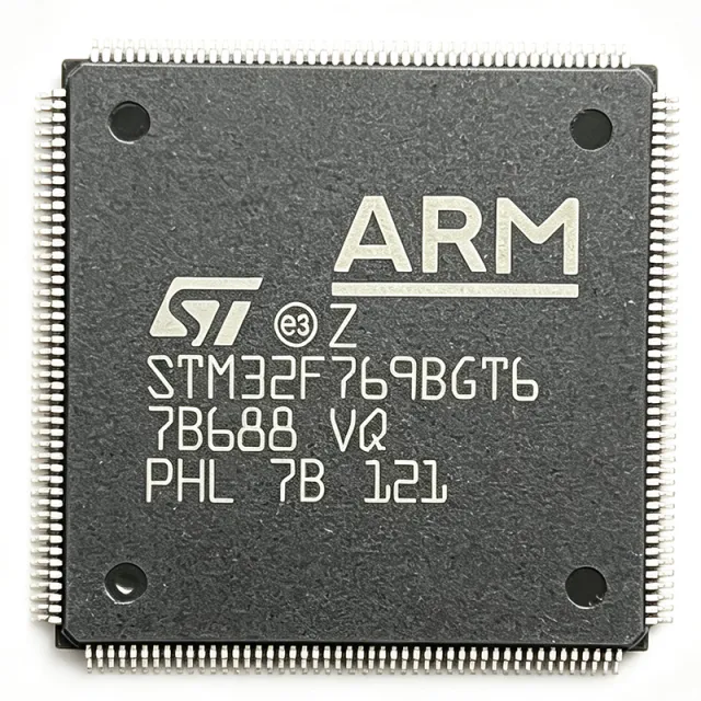
STM32F769BGT6 - 2MB Flash, 216MHz Cortex-M7 MCU | STMicroelectronics
STM32F769BGT6

STM32F769BGT6 - 2MB Flash, 216MHz Cortex-M7 MCU | STMicroelectronics

The STMicroelectronics STM32F769BGT6 is a high-performance ARM Cortex-M7 microcontroller with a double-precision FPU, operating at up to 216 MHz. It integrates 2 MB of Flash and 512 KB of SRAM, and is housed in a 208-pin LQFP package (TFBGA/LQFP208 family) supporting TFT-LCD, Ethernet, USB, and hardware cryptography for graphics-rich secure embedded designs. What is a microcontroller? A microcontroller (MCU) is a compact integrated circuit that combines a processor core, volatile memory (SRAM), non-volatile memory (Flash), and programmable input/output peripherals on a single chip. Microcontrollers are the backbone of embedded systems, ranging from simple household appliances to complex industrial automation. The STM32F769BGT6 belongs to the STM32F7 series within the broader STM32 family of 32-bit ARM Cortex-M microcontrollers, placing it in the high-performance segment with advanced connectivity, hardware crypto, and TFT graphics. Key specifications include a Chrom-ART Accelerator that offloads 2D DMA transfers from the CPU, an integrated TFT-LCD controller supporting resolutions up to WXGA, an 8 KB instruction cache and 8 KB data cache for low-latency code execution, and a hardware cryptographic accelerator plus True Random Number Generator (TRNG) for secure-boot and TLS applications. Operating voltage spans 1.7 V to 3.6 V across the industrial -40 °C to +85 °C range. Technically, the device is fabricated on a low-power 40 nm CMOS process and includes the M7 instruction cache, DTCM and AXI/AHB bus matrix, DSP extensions, and the STM32 standard library ecosystem (HAL/LL drivers, STM32CubeMX). External memory interfaces include FMC for SDRAM, NOR/NAND Flash, and SRAM expansion. This architecture cleanly separates code, data, and peripheral DMA traffic. Typical applications include human-machine interface (HMI) panels with TFT displays, industrial PLCs, secure IoT gateways, point-of-sale terminals, motor-control drives, and medical imaging controllers. The combination of high clock speed, hardware crypto, and Ethernet MAC makes it ideal for connected, secure, graphics-rich products. When designing with this LQFP-208 device, follow ST's recommended land pattern and use a 4-layer PCB with a solid ground plane for the high-speed SDMMC, USB, and Ethernet signals. Provide dedicated 100 nF + 4.7 µF decoupling on each VDD pin, keep the NRST reset trace short, and ensure the BYPASS_REG pin uses a 1 nF + 1 µF network for internal LDO stability. This page synthesizes distributor pricing, drop-in alternatives, application companions, and practical design notes beyond the manufacturer datasheet to accelerate your BOM and firmware decisions.

USD $17.92 Contact
STM32F769BIT6 - Cortex-M7 MCU 2MB Flash 216MHz LQFP-208 | ST
STM32F769BIT6

STM32F769BIT6 - Cortex-M7 MCU 2MB Flash 216MHz LQFP-208 | ST

The STMicroelectronics STM32F769BIT6 is a high-performance ARM Cortex-M7 32-bit RISC microcontroller with FPU and DSP instructions, operating at up to 216 MHz and delivering 462 DMIPS / 1082 CoreMark performance, packaged in a 208-pin LQFP (28x28 mm). It integrates 2 MB of Flash and 512 KB of SRAM, with an additional 16 KB instruction cache plus 16 KB I-cache for tight-memory code acceleration, making it one of the most capable Cortex-M7 MCUs in the STM32F7 family. What is a Cortex-M7 microcontroller? A microcontroller (MCU) is a single-chip computer containing a CPU core, Flash program memory, SRAM data memory, and a wide set of on-chip peripherals such as ADCs, timers, communication controllers and GPIOs. The ARM Cortex-M7 is the highest-performance core in the Cortex-M family, featuring a 6-stage superscalar pipeline, branch prediction, single/double-precision FPU, and tightly-coupled memories. It targets DSP-rich applications, advanced HMI graphics, and high-speed data acquisition where a Cortex-M4/M33 would lack throughput. The STM32F769BIT6 sits in the high-end tier of the STM32 line (LDO → microcontroller → embedded processor → semiconductor). Key features include an integrated Chrom-ART Accelerator 2D graphics engine, a hardware JPEG codec, dual QSPI/OctoSPI interfaces for external Flash expansion, a TFT-LCD controller up to WXGA, three 12-bit ADCs (2.4 MSPS each), two 12-bit DACs, USB 2.0 OTG FS + HS with on-chip PHY, Ethernet MAC, SDMMC, CAN, I2C, SPI/I2S, UART/USART, and a cryptographic/hash accelerator. The LQFP-208 package exposes up to 168 GPIOs and offers ample headroom for parallel-display, camera (DCMI), and SDRAM-bus expansion designs. Typical applications include advanced HMI panels with TFT-LCD and touch, industrial control and PLC front-ends, smart-home gateways, barcode scanners and label printers, audio DSP front-ends with the SAI/DFSDM peripherals, motor-control FOC platforms, and point-of-sale terminals. The wide peripheral set makes the STM32F769BIT6 a frequent choice when engineers need both graphics and deterministic real-time behavior in a single MCU. When designing with this part, pay attention to the BYPASS_REG and VCAP pins: the integrated SMPS step-down regulator of the F7 series requires two external capacitors on each VCAP pin for the 1.1V core rail, and the BYPASS_REG pin must be tied correctly to select internal-regulator or external-supply mode. Decoupling should follow ST's AN4661 guidance (multiple 100 nF plus bulk 4.7 µF per supply rail). This page synthesizes distributor pricing, drop-in LQFP-208 alternatives from ST and cross-brand options, and engineering-grade selection notes that complement - but do not replace - the manufacturer datasheet.

RFQ Contact
STM32F769IGT6 - 216MHz Cortex-M7 MCU, 1MB Flash | STMicroelectronics
STM32F769IGT6

STM32F769IGT6 - 216MHz Cortex-M7 MCU, 1MB Flash | STMicroelectronics

The STMicroelectronics STM32F769IGT6 is a high-performance 32-bit ARM Cortex-M7 microcontroller with FPU and DSP instructions, integrating 1 MB of Flash and 340 + 256 KB SRAM in a 176-pin LQFP (24x24 mm) package. The Cortex-M7 core delivers up to 216 MHz clock speed with 462 DMIPS and supports single-precision floating-point, double-precision FPU, and full DSP/MPU instruction set for signal processing workloads. What is a Cortex-M7 microcontroller? The Cortex-M7 is Arm's highest-performance microcontroller core for embedded applications, designed for real-time control and DSP. It sits in the hierarchy as: Cortex-M7 -> ARM Cortex-M family -> 32-bit MCU -> microcontroller -> semiconductor. The STM32F7 series integrates this core with large SRAM, hardware graphics (Chrom-ART accelerator, JPEG codec), and rich connectivity, making it suitable for high-end HMI, audio, and motor control. Key features of the STM32F769IGT6 include: 1 MB Flash with dual-bank architecture for live firmware upgrades, up to 2 MB external memory expansion via FMC (Flexible Memory Controller), 16-bit ADCs (up to 3 MSPS), two CAN 2.0B interfaces, USB OTG full-speed + USB OTG high-speed with on-chip HS PHY, two SDMMC interfaces, TFT-LCD controller, and the Chrom-ART graphics accelerator. The 176-LQFP exposes the maximum peripheral set of the F7 series, including 8-bit/16-bit FSMC, SAI audio interfaces, and SPDIF-Rx. Architecturally, the STM32F769IGT6 uses an advanced 90 nm process with an adaptive real-time ART Accelerator that delivers zero-wait-state execution from Flash at full 216 MHz. Multi-layer AHB/APB bus matrix, 16 DMA streams with FIFOs, and a dedicated DMA2D engine for image data transfer accelerate data movement. The MCU operates at 1.7-3.6 V with selectable LDO/SMPS regulator (BYPASS_REG pin) and includes a real-time clock, watchdog, and SysTick. Primary applications are high-end human-machine interface (HMI) panels, smart-home gateways, motor drives, professional audio, point-of-sale terminals, and embedded graphics with TFT-LCD + touch. The integrated TFT-LCD controller and JPEG codec remove the need for an external graphics MCU in many designs. Design consideration: the LQFP-176 package is large (24x24 mm) and requires careful PCB layout for the high-speed USB HS, SDMMC, and external memory interfaces. Use impedance-controlled traces for USB and RMII, and isolate analog/digital grounds. This page synthesizes distributor pricing, drop-in same-package alternatives (STM32F767IIT6 with 2 MB Flash, STM32F765IGT6), and practical design notes not found in the manufacturer datasheet alone.

RFQ Contact
STM32F769NIH6 - 2MB Flash 216MHz ARM Cortex-M7 MCU | STMicroelectronics
STM32F769NIH6

STM32F769NIH6 - 2MB Flash 216MHz ARM Cortex-M7 MCU | STMicroelectronics

The STMicroelectronics STM32F769NIH6 is a high-performance ARM Cortex-M7 microcontroller operating at up to 216 MHz, delivering 462 DMIPS/2.14 DMIPS/MHz, with 2 MB of dual-bank Flash and 512 KB of SRAM in a 216-pin TFBGA (13x13 mm) package. It supports 1.7V to 3.6V supply and -40C to +85C industrial temperature range, integrating a TFT LCD controller, hardware JPEG codec, and Chrom-ART Accelerator for graphics-rich applications. What is a microcontroller? A microcontroller (MCU) is a compact integrated circuit that combines a processor core, Flash/SRAM memory, and programmable I/O peripherals on a single die, governing a defined operation in an embedded system. The STM32F769NIH6 belongs to the STM32F7 series within the broader STM32 family of 32-bit Flash microcontrollers. The hierarchy STM32F769 -> STM32F7 -> STM32 -> ARM Cortex-M7 places it in the high-performance tier with DSP extensions and a single-precision floating-point unit (FPU). Cortex-M7 MCUs are the preferred choice for real-time signal processing, motor control, advanced audio, and rich human-machine interface (HMI) systems that require both computational density and connectivity. Key features include the Chrom-ART Accelerator for offloading 2D DMA2D operations (up to 10x faster than software rendering), a TFT LCD controller supporting up to XGA resolution, a hardware JPEG codec, and a cryptographic acceleration unit. The device exposes 168 GPIO across multiple ports, four I2C, six SPI, four USART/UART, three CAN, two SAI audio interfaces, one SDMMC, two USB 2.0 OTG (HS+FS), and two Ethernet MAC controllers. External memory bus (FMC) supports SDRAM, SRAM, NOR, and NAND for large frame buffers and code overlays. The 40nm process technology provides a balanced performance-per-watt profile for industrial embedded designs. Technically, the STM32F769NIH6 includes the Cortex-M7 core with single-precision FPU, a memory protection unit (MPU), DSP instruction set, true random number generator (TRNG), real-time clock (RTC), and 12-bit ADCs/DACs. Two 12-bit DACs, three 12-bit ADCs, and seventeen timers (including 32-bit and 16-bit) enable precise motor control and audio synthesis. The external memory interface (FMC) supports PSRAM, NOR Flash, NAND Flash, and SDRAM, enabling up to 32-bit external buses with multiplexing. Typical applications include high-end consumer electronics, industrial HMI panels, point-of-sale terminals, medical devices, audio processing subsystems, motor drives, and IoT gateways. The STM32F769NIH6 is particularly well-suited for smart home control panels and industrial displays where its graphics acceleration, JPEG codec, and Ethernet/USB connectivity deliver a complete platform. When designing with this device, ensure proper decoupling with 100nF capacitors placed close to each VDD pin, and provide a 25 MHz HSE oscillator and a 32.768 kHz LSE crystal for RTC. For USB HS and Ethernet, route the differential pairs with 90-dpi impedance and use the internal PLL to derive 48 MHz. Hold NRST low during power-up and ensure VDD is applied before VDDA per datasheet sequencing guidelines. This page synthesizes distributor pricing, drop-in alternatives from the same STM32F7 family, and practical design notes not aggregated on manufacturer product pages.

RFQ Contact
STM32F777BIT6 - 2MB Flash, 216MHz ARM Cortex-M7 MCU | STMicroelectronics
STM32F777BIT6

STM32F777BIT6 - 2MB Flash, 216MHz ARM Cortex-M7 MCU | STMicroelectronics

The STMicroelectronics STM32F777BIT6 is a high-performance ARM Cortex-M7 based microcontroller operating at up to 216 MHz, delivering 462 DMIPS and 1082 CoreMark. It features 2 MB of dual-bank Flash memory and 512 KB of SRAM, making it suitable for complex embedded applications requiring substantial code and data storage. The device is housed in a 208-pin LQFP (LQFP208) package with a 28x28 mm body and 0.5 mm pitch, providing ample I/O for system integration. What is a microcontroller? A microcontroller (MCU) is a compact integrated circuit designed to govern a specific operation in an embedded system. It integrates a processor core, memory (Flash and SRAM), and programmable input/output peripherals on a single chip. Microcontrollers are the foundation of modern embedded systems, ranging from automotive engine control units to consumer IoT devices. The STM32F7 series sits at the high-performance tier of the STM32 family, positioned above the mainstream STM32F4 series and below the higher-end STM32H7 series, offering a balance of performance, memory, and peripheral integration. Key features include a Chrom-ART Accelerator for 2D graphics, a hardware cryptographic processor supporting AES, DES, 3DES, and hash functions, and a true random number generator (TRNG). The device also integrates a TFT LCD controller, a JPEG codec, and a camera interface, enabling rich human-machine interfaces. With 168 MHz maximum ADC conversion rate and multiple communication interfaces including Ethernet MAC, USB OTG HS, and CAN, the STM32F777BIT6 is designed for connectivity-intensive applications. Technically, the STM32F777BIT6 is built on a 40 nm process technology, offering low power consumption with multiple low-power modes: Sleep, Stop, and Standby. The dual-bank Flash allows read-while-write operations, enabling firmware updates without halting the system. The device supports external memory interfaces for SDRAM, SRAM, and NOR/NAND Flash, expanding memory beyond the on-chip resources. The Chrom-ART accelerator offloads 2D graphics operations from the CPU, improving GUI performance while reducing power consumption. Typical applications include industrial control systems, medical devices, smart home hubs, and high-end consumer electronics. The combination of high CPU performance, rich connectivity, and advanced security features makes it ideal for applications requiring real-time processing, secure communication, and graphical user interfaces. For example, in an industrial HMI, the STM32F777BIT6 can drive a TFT display, handle Ethernet communication, and execute control algorithms simultaneously. When designing with this device, ensure adequate decoupling on all power supply pins and a proper ground plane for the LQFP208 package. The high-speed peripherals, such as Ethernet and USB, require careful PCB layout to maintain signal integrity. Also, consider the thermal dissipation of the 216 MHz core; a thermal pad or heatsink may be necessary for sustained high-load operation.

RFQ Contact
STM32F777IIK6 - 216MHz Cortex-M7 MCU 2MB Flash UFBGA-176 | STMicroelectronics
STM32F777IIK6

STM32F777IIK6 - 216MHz Cortex-M7 MCU 2MB Flash UFBGA-176 | STMicroelectronics

The STMicroelectronics STM32F777IIK6 is a high-performance 32-bit ARM Cortex-M7 microcontroller with FPU and DSP extensions, operating at 216 MHz and delivering up to 462 DMIPS / 1084 CoreMark performance. The device integrates 2 MB of dual-bank Flash memory, 512 KB of SRAM (with 16 KB and 4 KB sub-banks for backup and CCM), advanced cryptographic accelerators (AES, Hash, true-RNG), and a TFT-LCD + DSI controller, all housed in a 176-pin UFBGA package (10x10 mm). A microcontroller (MCU) is a system-on-chip that integrates a CPU core, memory, peripherals, and dedicated hardware accelerators into a single die. The ARM Cortex-M class targets deterministic, energy-efficient embedded control; the Cortex-M7 specifically adds a double-precision FPU, branch prediction, and tightly-coupled instruction/data memories (ICACHE/DCACHE), enabling DSP workloads and high-throughput GUI rendering on a low-power platform. Within ST's families, the STM32F777 sits in the high-end F7 line, with the F777IIK6 suffix denoting 2 MB Flash, 176-pin UFBGA (industrial temperature range, tray packaging). Key features include 216 MHz CPU speed, 32-channel DMA, two 12-bit ADCs (up to 2.4 MSPS each), two 12-bit DACs, low-power RTC, two USB OTG interfaces (HS and FS), 10/100 Ethernet MAC, three CAN 2.0B controllers, USB Power Delivery support, HDMI-CEC hardware, SDMMC, dual-mode Quad-SPI, and an external memory bus for SDRAM/NAND/NOR. The TFT-LCD and MIPI-DSI controllers make this part well-suited for advanced graphical HMIs without an external display controller. Architecturally, the STM32F777 is built on a 90 nm CMOS process with an ART Accelerator allowing zero-wait-state execution from Flash, four I2S/SAI interfaces for audio, six SPIs, four I2Cs, five USARTs/UARTs, and two UARTs dedicated to low-power modes. Crypto/hash hardware (AES 128/192/256, SHA-1/SHA-2) and a unique 96-bit device ID support secure boot and signed firmware. The 176+25 UFBGA pinout exposes all peripherals simultaneously and provides strong power/ground integrity for the high-speed interfaces. Typical applications include industrial HMI panels, smart appliances with rich GUIs, point-of-sale terminals, machine-vision controllers, USB Type-C audio docks, and medical instruments with graphic displays. The external memory interface and dual-mode QSPI enable fast external NOR or PSRAM expansion for in-field firmware upgrades or large display buffers. When designing with this part, dedicate a solid ground pour on the top layer to manage the 216 MHz core current transients and keep the VDD/VDDA decoupling capacitors within 2 mm of their respective pins. The DSI lanes require length matching within 50 mils to maintain signal integrity. This page synthesizes distributor pricing, drop-in STM32F7 alternatives, and practical design notes from the STM32F777xx datasheet not consolidated on any single distributor page.

RFQ Contact
STM32F777IIT6 - 216MHz Cortex-M7 MCU, 2MB Flash | ST
STM32F777IIT6

STM32F777IIT6 - 216MHz Cortex-M7 MCU, 2MB Flash | ST

The STMicroelectronics STM32F777IIT6 is a high-performance 32-bit Arm Cortex-M7 microcontroller operating up to 216 MHz, with 2 MB of Flash memory, 512 KB of SRAM, and a 176-pin LQFP package measuring 24 x 24 mm. It combines a high-speed microcontroller core, extensive peripheral connectivity, and industrial-temperature component qualification in a surface-mount package. A microcontroller is a programmable integrated circuit containing a processor core, memory, and peripherals that together implement a complete embedded control function. Within the semiconductor hierarchy, an MCU is a system-on-chip type of integrated circuit used for real-time control, signal processing, communications, and automation. The STM32F7 series occupies the high-performance segment of the STM32 product family and targets demanding embedded applications. Principal device characteristics include a 216 MHz Cortex-M7 core, 2 MB of Flash, 512 KB of SRAM, dual-mode Quad-SPI, and support for up to 18 timers. The timer configuration includes thirteen 16-bit timers, two 32-bit timers, and additional timer channels for input capture, output compare, PWM generation, pulse counting, and incremental-encoder interfaces. Two watchdogs and the SysTick timer support reliable background and operating-system timing functions. The STM32F777 device family combines substantial memory bandwidth with a large pin count, allowing simultaneous use of high-speed communications, display interfaces, analog peripherals, and general-purpose I/O. Its 176-LQFP package provides extensive external connectivity while avoiding the mechanical complexity of a ball-grid array. The STM32F777IIT6 ordering code identifies the 176-pin LQFP configuration and the industrial temperature option. Typical applications include industrial automation controllers, high-speed communications equipment, motor-control systems, audio and digital signal processing platforms, human-machine interfaces, and networked embedded products. The 216 MHz Cortex-M7 core is particularly useful when workloads require deterministic real-time response alongside extensive peripheral integration. PCB design should follow the manufacturer's land-pattern and pin-definition guidance exactly. Keep high-speed clock and communication traces short, provide the specified bypass capacitors near their supply pins, and verify that exposed test points and programming access remain compatible with the assembled board. Firmware selection, boot configuration, clock-tree setup, and peripheral initialization should be validated against the device datasheet and reference documentation. This product summary consolidates the core electrical specifications, package details, same-family alternatives, interface considerations, and practical design guidance into one engineering reference. It also distinguishes direct STM32F7 options from products that may require firmware, peripheral, or PCB validation before substitution.

RFQ Contact
STM32F777VIT6 - 216MHz Cortex-M7 MCU | STMicroelectronics
STM32F777VIT6

STM32F777VIT6 - 216MHz Cortex-M7 MCU | STMicroelectronics

STMicroelectronics STM32F777VIT6 is a 32-bit Arm Cortex-M7 microcontroller operating at up to 216 MHz, with 2 MB of Flash memory and 512 KB of RAM in a 100-pin LQFP package measuring 14 x 14 mm. It combines high-performance embedded processing with extensive serial connectivity and timer resources for demanding industrial control, communications, audio, and real-time embedded applications. A microcontroller is a programmable semiconductor that integrates a processor core, memory, peripherals, and communication interfaces on one device. The STM32F7 family belongs to the Arm Cortex-M product hierarchy, where the STM32F777VIT6 combines a 32-bit RISC core, embedded Flash, SRAM, timers, serial controllers, and GPIO. This integration reduces system complexity by placing control, data acquisition, communications, and real-time processing within a single package. The STM32F777VIT6 reaches a maximum core frequency of 216 MHz and provides 2 MB of Flash plus 512 KB of SRAM. Its timer configuration includes as many as 18 timers, including up to 13 16-bit timers, two 32-bit timers, two watchdogs, and the SysTick timer. According to the STMicroelectronics datasheet, all 15 main timers can operate at up to 216 MHz, supporting precise timing, motor control, signal generation, and industrial automation functions. The device uses the Arm Cortex-M7 architecture with single-precision floating-point capability and a high-performance instruction set suited to control loops and digitally assisted signal processing. Dual-mode Quad-SPI support is also identified in the product documentation. These resources allow software to handle communications protocols, data acquisition, and control algorithms without relying on multiple discrete processing components. Typical uses include industrial motor controllers, factory automation nodes, high-performance human-machine interfaces, embedded audio equipment, communications gateways, and sensor-processing systems. The 100-LQFP package is particularly appropriate for prototypes, industrial controllers, and medium-complexity boards where a large pin count provides access to peripherals while remaining compatible with conventional leaded-package assembly processes. Power-supply design should preserve clean, stable rails for both the core and I/O domains, while high-speed communication interfaces require controlled impedance routing and short return paths. Firmware should also account for internal versus external clock selection, flash wait-state configuration, peripheral clock enablement, and the device-specific startup sequence described in the manufacturer reference manual. This product page combines core specifications, same-footprint replacement options, interface-oriented application guidance, and practical design cautions. It is intended to accelerate engineering evaluation while directing pin assignments, firmware support, and assembly decisions back to the authoritative STMicroelectronics datasheet and reference documentation.

RFQ Contact
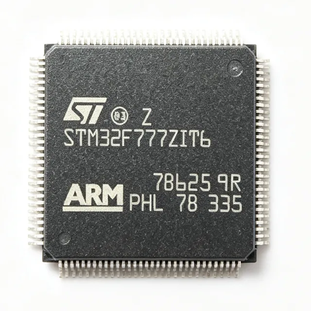
STM32F777ZIT6 - 2MB Flash, 216MHz ARM Cortex-M7 MCU | STMicroelectronics
STM32F777ZIT6

STM32F777ZIT6 - 2MB Flash, 216MHz ARM Cortex-M7 MCU | STMicroelectronics

The STMicroelectronics STM32F777ZIT6 is a high-performance ARM Cortex-M7 based microcontroller operating at up to 216 MHz, delivering 462 DMIPS and 1082 CoreMark. It features 2 MB of dual-bank Flash memory and 512 KB of SRAM, making it suitable for complex real-time applications. The device is housed in a 144-pin LQFP (ZIT) package with a 20x20 mm footprint, offering extensive I/O and connectivity options. What is a microcontroller? A microcontroller (MCU) is a compact integrated circuit designed to govern a specific operation in an embedded system. It integrates a processor core, memory (Flash and SRAM), and programmable input/output peripherals on a single chip. In the system hierarchy, an MCU sits above a bare microprocessor by including on-chip memory and peripherals, and below a full application processor (like those in smartphones) which typically runs a rich OS. The STM32F777ZIT6 belongs to the STM32F7 series, which is part of the broader STM32 family of 32-bit Flash microcontrollers based on ARM Cortex-M cores. This family is widely used in industrial, consumer, and IoT applications due to its balance of performance, power efficiency, and peripheral integration. Key features include a Chrom-ART Accelerator for 2D graphics, a hardware cryptographic accelerator (AES, DES, 3DES, SHA-1, SHA-256, MD5), a true random number generator, and a JPEG codec. The device supports a comprehensive set of communication interfaces: 4x I2C, 4x USART, 4x UART, 6x SPI, 3x CAN, 2x USB OTG (FS/HS), 2x SDMMC, 1x FMC (external memory interface), and 2x SAI (serial audio interfaces). It also includes a 12-bit ADC with 3.6 MSPS, a 12-bit DAC, and multiple timers including high-resolution timers. The STM32F777ZIT6 operates from a 1.7V to 3.6V supply and features a wide temperature range of -40°C to +85°C (industrial grade). It supports various low-power modes (Sleep, Stop, Standby) to optimize energy consumption. The device is RoHS compliant and available in tape and reel packaging. Typical applications include industrial control systems, motor drives, medical devices, audio processing, and high-end consumer electronics. The dual-bank Flash allows over-the-air firmware updates with minimal downtime, and the cryptographic accelerator enables secure communication protocols. When designing with this MCU, ensure adequate decoupling on all power pins and follow the recommended layout for the high-speed USB and external memory interfaces. The internal LDO can be bypassed for lower power consumption, but this requires careful power sequencing.

USD $22.59 Contact
STM32F779BIT6 - 32-bit ARM Cortex-M7 MCU, 2MB Flash, 216MHz | STMicroelectronics
STM32F779BIT6

STM32F779BIT6 - 32-bit ARM Cortex-M7 MCU, 2MB Flash, 216MHz | STMicroelectronics

The STM32F779BIT6 is a high-performance 32-bit microcontroller from STMicroelectronics, based on the ARM Cortex-M7 core running at up to 216 MHz. It features 2 MB of Flash memory and 512 KB of SRAM, making it suitable for complex applications requiring substantial code and data storage. The device is housed in a 208-pin LQFP package (LQFP208) with a 28x28 mm body, offering a rich set of peripherals and I/O capabilities. A microcontroller (MCU) is a compact integrated circuit designed to govern a specific operation in an embedded system. It contains a processor core, memory (Flash and SRAM), and programmable input/output peripherals. The STM32F779BIT6 belongs to the STM32F7 series, which is part of the broader STM32 family of 32-bit ARM Cortex-M microcontrollers. This family is widely used in industrial, consumer, and automotive applications due to its balance of performance, power efficiency, and peripheral integration. Key features include a 216 MHz Cortex-M7 core with double-precision FPU, 2 MB Flash, 512 KB SRAM, and a comprehensive set of peripherals: multiple 12-bit ADCs, DACs, timers, communication interfaces (USART, SPI, I2C, CAN, USB OTG, Ethernet MAC), and advanced security features like cryptographic acceleration and true random number generator. The device also supports external memory interfaces (FMC) for SDRAM, NOR, and NAND Flash expansion. The STM32F779BIT6 leverages the ARM Cortex-M7 architecture with a 6-stage pipeline and a branch prediction unit, delivering 2.14 CoreMark/MHz. It includes a hardware cryptographic accelerator (AES, DES, 3DES, SHA-1, SHA-256) and a true random number generator (TRNG), enhancing security for IoT and connectivity applications. The device operates from 1.7V to 3.6V supply, with multiple low-power modes (Sleep, Stop, Standby) for energy-sensitive designs. Typical applications include industrial control systems, motor drives, IoT gateways, audio processing, and high-end consumer electronics. The rich peripheral set and high clock speed make it ideal for real-time control and signal processing tasks. The FMC interface allows seamless connection to external memory, expanding storage for data logging or graphical user interfaces. When designing with this MCU, ensure proper decoupling of the power supply pins with 100 nF capacitors placed close to each VDD pin, and a 4.7 uF bulk capacitor. The VDDA analog supply should be filtered with a ferrite bead and 1 uF capacitor to reduce noise for ADC accuracy. The BOOT0 pin configuration must be set correctly for desired boot mode (Flash, System memory, or SRAM).

RFQ Contact
STM32F779NIH6 - 216MHz Cortex-M7 MCU, 2MB Flash, 216-TFBGA | STMicroelectronics
STM32F779NIH6

STM32F779NIH6 - 216MHz Cortex-M7 MCU, 2MB Flash, 216-TFBGA | STMicroelectronics

The STMicroelectronics STM32F779NIH6 is a high-performance 32-bit ARM Cortex-M7 microcontroller running at up to 216 MHz with 2 MB of embedded Flash and 512 KB of SRAM, housed in a 216-ball TFBGA (13x13 mm) package. It integrates an Arm Cortex-M7 core with double-precision FPU, 16 KB I-cache / 16 KB D-cache, ART Accelerator for 0-wait-state execution, MPU, 462 DMIPS (2.14 DMIPS/MHz, Dhrystone 2.1), and DSP instructions. Peripherals include high-speed USB OTG, Ethernet MAC, SDMMC, FMC, Quad-SPI, and an on-chip crypto/hash block in select derivatives. An ARM Cortex-M7 microcontroller is a 32-bit RISC processor core from Arm's Cortex-M family that targets high-performance embedded applications requiring DSP and floating-point capabilities. Cortex-M7 sits at the top of the Cortex-M hierarchy (Cortex-M7 -> Cortex-M -> Arm architecture -> 32-bit MCU) and supersedes Cortex-M4 by adding a 6-stage superscalar pipeline, dual-issue load/store, branch prediction, and optional double-precision FPU. Compared to Cortex-M4 parts, Cortex-M7 MCUs typically deliver 2x DSP performance and 1.5-2x integer performance at similar clock rates. Key features of the STM32F779NIH6 include the ART Accelerator enabling 0-wait-state flash execution at 216 MHz, dedicated instruction and data caches, a Chrome-ART graphics accelerator for TFT-LCD and MIPI-DSI interfaces, hardware crypto acceleration (AES, SHA, DES, RNG), multiple 12-bit ADCs (2.4 MSPS), two 12-bit DACs, and up to 18 timers including 32-bit and motor-control variants. The device supports USB 2.0 high-speed OTG, two CAN 2.0B controllers, an Ethernet MAC with IEEE 1588, SDMMC, and Quad-SPI for external serial memory expansion. Typical applications for the STM32F779NIH6 span industrial HMI with TFT-LCD and touch, motor control (BLDC/PMSM), high-end audio processing with DSP, networked IoT gateways, point-of-sale terminals, and graphical embedded products. The wide peripheral set and 2 MB flash also make it suitable for secure connected devices using the on-chip hardware crypto engine. When designing with the STM32F779NIH6, ensure the 216-ball TFBGA is compatible with your PCB manufacturing capabilities. Use ST's STM32CubeMX and STM32CubeIDE for pin mux configuration, code generation, and debugging. Pay attention to decoupling (place 100 nF + 4.7 uF near each VDD pin pair), JTAG/SWD trace layout for debug, and boot-mode pin straps for flash programming.

RFQ Contact
STM32F779ZIT6 - 2MB Flash, 216MHz Cortex-M7 MCU | STMicroelectronics
STM32F779ZIT6

STM32F779ZIT6 - 2MB Flash, 216MHz Cortex-M7 MCU | STMicroelectronics

The STMicroelectronics STM32F779ZIT6 is a high-performance ARM Cortex-M7 based microcontroller with a 32-bit core running at up to 216 MHz. It features 2 MB of Flash memory and 512 KB of SRAM, making it suitable for complex applications requiring substantial code and data storage. The device is housed in a 144-pin LQFP package (LQFP144) with a 20x20 mm body and 0.5 mm pitch, offering a compact yet high-density solution for advanced embedded systems. What is a microcontroller? A microcontroller (MCU) is a compact integrated circuit designed to govern a specific operation in an embedded system. It integrates a processor core, memory (Flash and SRAM), and programmable input/output peripherals on a single chip. Microcontrollers are the backbone of modern electronics, found in automotive engine control units, industrial automation, consumer appliances, and IoT devices. They sit within the broader hierarchy of embedded systems, which include sensors, actuators, and communication interfaces, all coordinated by the MCU's processing capabilities. Key features of the STM32F779ZIT6 include a rich set of peripherals: multiple 12-bit ADCs, DACs, timers, USARTs, SPIs, I2Cs, USB OTG, Ethernet MAC, camera interface, and a Chrom-ART Accelerator for graphics. It also integrates a hardware cryptographic processor supporting AES, DES, and 3DES, along with a true random number generator (TRNG). The device supports a wide supply voltage range of 1.7V to 3.6V and operates over a temperature range of -40°C to +85°C (industrial grade). The STM32F779ZIT6 is built on ST's advanced 90nm process technology, enabling high clock speeds with low power consumption. The Cortex-M7 core features a 6-stage pipeline, branch prediction, and a single-precision floating-point unit (FPU), delivering 1082 CoreMark score at 216 MHz. The memory architecture includes an 8-Kbyte instruction cache and an 8-Kbyte data cache, reducing access latency and improving real-time performance. Typical applications include high-end consumer electronics, industrial control systems, medical devices, and IoT gateways. The combination of high performance, extensive connectivity, and security features makes it ideal for applications requiring advanced user interfaces, connectivity, and data processing. When designing with this device, ensure proper decoupling of the power supply pins with 100nF capacitors placed close to each VDD pin, and a bulk capacitor (e.g., 4.7uF) on the main supply. The VDDA pin must be connected to a clean analog supply to minimize ADC noise. Also, consider the thermal dissipation: the LQFP144 package has a thermal resistance of 40°C/W (theta_JA), so adequate PCB copper area is recommended for high-current applications.

RFQ Contact
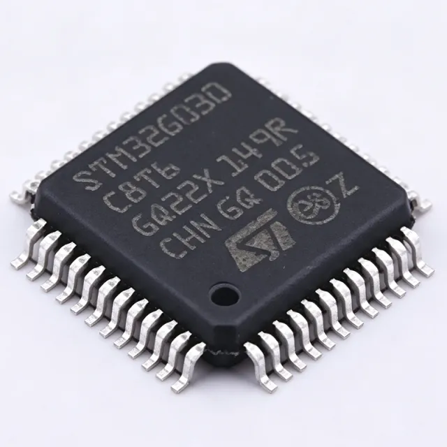
STM32G030C6T6 - Cortex-M0+ MCU, 64MHz, 32KB Flash, LQFP-48
STM32G030C6T6

STM32G030C6T6 - Cortex-M0+ MCU, 64MHz, 32KB Flash, LQFP-48

The STMicroelectronics STM32G030C6T6 is a 32-bit Arm Cortex-M0+ mainstream microcontroller operating at up to 64 MHz, offering 32 KB of Flash and 8 KB of SRAM in a 48-pin LQFP (7x7 mm) package. It is part of the STM32G0 value-line series designed for cost-sensitive embedded applications requiring modern peripherals and low power consumption. An Arm Cortex-M0+ microcontroller is a low-power 32-bit processor core based on the Armv6-M architecture, optimized for energy-efficient embedded designs. It belongs to the broader category of microcontrollers (MCUs), which integrate CPU, memory, and peripherals on a single die. The Cortex-M0+ sits below Cortex-M3/M4 in performance but excels at deterministic interrupt response and minimal energy per instruction, making it ideal for sensor nodes, human-machine interfaces (HMI), and battery-powered consumer devices. The STM32G0 family represents ST's entry-level mainstream line, balancing 8-bit MCU cost with 32-bit performance. Key features include the Cortex-M0+ core with single-cycle I/O access, hardware CRC, real-time clock, low-power Run/Stop/Standby/Shutdown modes, and an operating temperature range of -40C to +85C. The device integrates an 11-channel 12-bit ADC (2.5 Msps), multiple timers, and serial interfaces including USART, SPI, and I2C (with Fast-mode Plus support up to 1 Mbit/s). The integrated voltage regulator and brown-out reset simplify power-supply design across 2.0V to 3.6V supplies. Technical depth: the STM32G030C6T6 uses ST's 90 nm process with on-chip voltage scaling, achieving typical Run-mode current under 1 mA/MHz and Stop-mode current in the microamp range. The single-wire debug (SWD) interface and integrated bootloader shorten firmware bring-up. Hardware parity on SRAM catches single-bit faults in safety-relevant code. Typical applications include small appliance controls, USB Type-C cable marker ICs, simple HMI panels (buttons, LEDs), and sensor hubs. The wide operating voltage allows direct battery connection in 2xAA or coin-cell systems. Design consideration: leverage the LQFP-48 (7x7 mm) package's exposed pad for thermal relief; if unused, leave it floating or stitch to ground per ST's design recommendations. This page combines authoritative ST datasheet data, drop-in alternates, and practical design notes to support engineer selection and second-sourcing decisions.

RFQ Contact
STM32G030C8T6 - 64KB Flash ARM Cortex-M0+ MCU | STMicroelectronics
STM32G030C8T6

STM32G030C8T6 - 64KB Flash ARM Cortex-M0+ MCU | STMicroelectronics

The STM32G030C8T6 is a 32-bit ARM Cortex-M0+ based microcontroller from STMicroelectronics, featuring 64KB of Flash memory and 8KB of SRAM. It operates at a maximum clock frequency of 64 MHz and is housed in a 48-pin LQFP package (7x7 mm). This device is part of the STM32G0 series, designed for cost-sensitive and power-efficient applications. What is a microcontroller? A microcontroller (MCU) is a compact integrated circuit containing a processor core, memory, and programmable input/output peripherals on a single chip. It is the brain of embedded systems, executing instructions to control devices such as sensors, motors, and displays. In the system hierarchy, a microcontroller falls under embedded processors, which are part of the broader category of integrated circuits. The STM32G030C8T6 is a mainstream MCU, balancing performance, power consumption, and cost for a wide range of applications. Key features include a 12-bit ADC with up to 19 channels, multiple timers (including advanced-control timers), and a rich set of communication interfaces: I2C, SPI, USART, and low-power UART. The device supports a supply voltage range of 2.0V to 3.6V and offers multiple low-power modes (Sleep, Stop, Standby) to optimize energy consumption. It also includes a DMA controller, CRC calculation unit, and a real-time clock (RTC). The STM32G030C8T6 is built on a high-performance ARM Cortex-M0+ core with a single-cycle multiplier and a nested vectored interrupt controller (NVIC). It features a memory protection unit (MPU) for enhanced security and reliability. The device is supported by ST's comprehensive ecosystem, including the STM32CubeMX configuration tool and the STM32CubeG0 firmware library, which accelerate development. Typical applications include industrial control systems, consumer electronics, IoT devices, home automation, and battery-powered equipment. Its low power consumption and rich peripheral set make it suitable for sensor hubs, motor control, and human-machine interfaces (HMI). When designing with this MCU, ensure proper decoupling of the power supply pins with 100nF capacitors placed close to the VDD pins. For low-power applications, utilize the Stop and Standby modes to reduce current consumption to microamp levels. The device is RoHS compliant and available in tape and reel packaging for automated assembly.

USD $1.47 Contact
STM32G030F6P6 - 64MHz Cortex-M0+ MCU, 32KB Flash | STMicroelectronics
STM32G030F6P6

STM32G030F6P6 - 64MHz Cortex-M0+ MCU, 32KB Flash | STMicroelectronics

The STM32G030F6P6 is a mainstream 32-bit microcontroller from STMicroelectronics, built on the high-performance Arm® Cortex®-M0+ RISC core operating at up to 64 MHz. It features 32 KB of Flash memory and 8 KB of SRAM with hardware parity, housed in a compact 20-pin TSSOP package. This device is designed for cost-sensitive, mass-production applications, offering a balanced combination of performance, memory, and peripheral integration. What is a microcontroller (MCU)? A microcontroller is a compact integrated circuit designed to govern a specific operation in an embedded system. It integrates a processor core, memory (Flash and SRAM), and programmable input/output peripherals on a single chip. The STM32G030F6P6 belongs to the STM32G0 series, which is part of the broader STM32 family of 32-bit Arm Cortex-M microcontrollers. This hierarchy positions it as a mainstream, entry-level MCU within the STM32 ecosystem, ideal for applications ranging from simple control loops to more complex sensor and communication tasks. Key features of the STM32G030F6P6 include a 64 MHz Arm Cortex-M0+ core, 32 KB Flash, 8 KB SRAM, and a 2.0V to 3.6V supply range. It integrates a rich set of peripherals: I2C (with Fast-mode Plus up to 1 Mbit/s), USART, SPI, a 12-bit ADC, timers, and GPIOs. The device also supports a wide operating temperature range and is available in a 20-pin TSSOP package, making it suitable for space-constrained designs. Technically, the STM32G030F6P6 leverages the energy-efficient Cortex-M0+ architecture, which balances processing capability with low power consumption. The inclusion of hardware parity on SRAM enhances data integrity, a critical feature for safety-conscious applications. The I2C interface supports Standard-mode (100 kbit/s), Fast-mode (400 kbit/s), and Fast-mode Plus (1 Mbit/s), providing flexible communication options. The 12-bit ADC enables precise analog signal acquisition, essential for sensor-based applications. Typical applications include industrial control, consumer electronics, IoT devices, and simple automation systems. Its low cost and small footprint make it an excellent choice for high-volume products such as smart sensors, motor control, and portable devices. The wide supply voltage range and robust peripheral set ensure versatility across diverse use cases. When designing with this MCU, consider the 2.0V to 3.6V supply range and ensure proper decoupling with a 100nF capacitor close to each power pin. The 20-pin TSSOP package requires careful PCB layout to minimize noise, especially for the ADC and high-speed I2C lines. Refer to the STM32G030F6 datasheet for detailed electrical characteristics and recommended layout guidelines.

RFQ Contact
STM32G030J6M6 - 64MHz Cortex-M0+ 32KB Flash MCU | STMicroelectronics
STM32G030J6M6

STM32G030J6M6 - 64MHz Cortex-M0+ 32KB Flash MCU | STMicroelectronics

STMicroelectronics STM32G030J6M6 is an Arm Cortex-M0+ 32-bit microcontroller operating up to 64 MHz, with 32 KB of Flash memory, 8 KB of RAM, and six I/O pins in an 8-SOIC package. The device belongs to the STM32G0 mainstream value-line family and is positioned for compact, cost-sensitive embedded control designs that need efficient 32-bit processing without a large package. A microcontroller is a programmable semiconductor that integrates a CPU core, memory, peripheral interfaces, and I/O circuitry on one device. In the product hierarchy, the STM32G030J6M6 is an MCU, then a 32-bit microcontroller, then an embedded processor based on the Arm Cortex-M0+ architecture. This combination supports compact control logic, real-time peripheral operation, and efficient firmware execution in industrial, consumer, and embedded systems. Key features include a 64 MHz Arm Cortex-M0+ core, 32 KB Flash, 8 KB SRAM, and six I/O pins. The STM32G030 family provides I2C capability supporting Standard mode, Fast mode, and Fast mode Plus according to the manufacturer datasheet. The small SOIC package and six-pin I/O count are useful when board space is constrained, although the limited pin budget requires careful prioritization of communication, timing, and control signals. The STM32G030x6/x8 devices use the high-performance 32-bit Arm Cortex-M0+ RISC core. The M0+ architecture is designed for efficient embedded operation and supports deterministic control in applications where response time and power-conscious code execution are important. Compared with larger STM32 families, the G030 devices target mainstream value-line designs where 32 KB Flash and 8 KB RAM are sufficient for the product function. Typical uses include compact sensor-control boards, industrial automation modules, appliance controls, and low-cost communication peripherals. A designer should partition the six available I/O pins among required serial functions, control outputs, and interrupts, then verify that the selected peripheral multiplexing remains consistent with the board architecture. The principal design consideration is footprint planning. The 8-SOIC package simplifies assembly but offers only six I/O pins, so a design needing more external signals should consider a larger STM32G0 package rather than force costly signal multiplexing. Confirm power, decoupling, programming, reset, and clock requirements against the manufacturer datasheet before layout release. This product analysis combines the verified STMicroelectronics family data, distributor specifications, source documentation, and practical selection guidance into a concise engineering reference for cost-conscious embedded control applications.

RFQ Contact
STM32G030K6T6 64MHz 32KB MCU 32-LQFP | STMicroelectronics
STM32G030K6T6

STM32G030K6T6 64MHz 32KB MCU 32-LQFP | STMicroelectronics

The STMicroelectronics STM32G030K6T6 is a 32-bit Arm Cortex-M0+ microcontroller operating at up to 64 MHz, with 32 KB of Flash memory and 8 KB of SRAM, housed in a 32-LQFP 7 x 7 mm package. It belongs to the STM32G0 mainstream value line and combines a compact general-purpose MCU package with embedded memory and peripheral connectivity for embedded control designs. What is a microcontroller? A microcontroller is a semiconductor device that integrates a processor core, memory, and peripheral interfaces into one component. An Arm Cortex-M0+ core provides a compact, energy-efficient architecture for real-time control tasks, while the STM32G0 family sits within the broader hierarchy of microcontroller, embedded processor, semiconductor, and electronic-control component categories. The STM32G030K6T6 provides the verified headline resources of 64 MHz operating frequency, 32 KB Flash, and 8 KB SRAM. The 32-LQFP package exposes the device in a 7 x 7 mm surface-mount form factor suitable for compact control boards. Its mainstream value-line positioning makes it applicable to cost-sensitive embedded products where a small, general-purpose 32-bit MCU is sufficient. The Arm Cortex-M0+ processor architecture supports firmware-driven control without requiring a separate processor, while integrated Flash and SRAM reduce the number of external memory components in simpler designs. Exact peripheral counts, voltage limits, I/O ratings, and electrical timing values are not included in the supplied verified snippets and are therefore not asserted here. Typical application domains include industrial control, consumer electronics, small embedded controllers, sensor interfaces, and compact automation products. The verified product information identifies industrial control and consumer electronics as common applications, and the 64 MHz core and 32 KB memory footprint provide a clear platform for embedded logic, peripheral coordination, and control-loop software. Designers should verify the complete electrical limits, pin multiplexing, clock configuration, memory programming requirements, and package drawing in the official STMicroelectronics product documentation before layout release. For a purchase decision, compare the required peripheral mix and software ecosystem against the exact device revision and package variant. This product summary consolidates the verified manufacturer identity, distributor specifications, package information, and application context. Pricing and availability remain subject to distributor confirmation as of 2026-10-22, while detailed technical values not present in the supplied data are deliberately left for datasheet verification.

RFQ Contact
STM32G030K8T6 - 64MHz Cortex-M0+ MCU, 64KB Flash | ST
STM32G030K8T6

STM32G030K8T6 - 64MHz Cortex-M0+ MCU, 64KB Flash | ST

The STMicroelectronics STM32G030K8T6 is a mainstream 32-bit microcontroller based on an Arm Cortex-M0+ core running at up to 64 MHz, with 64 KB Flash memory and 8 KB SRAM, housed in a 32-pin LQFP (7x7 mm) package. An MCU (microcontroller unit) is a single-chip computer that integrates a processor core, program memory, data memory, and peripheral interfaces into one IC. Within the microcontroller hierarchy, the STM32G030K8T6 belongs to the STM32 mainstream value-line family, positioned as a cost-optimized entry point into the broader STM32 ecosystem and general-purpose embedded processor market. Key features include the high-performance Cortex-M0+ 32-bit RISC core at 64 MHz, 64 KB of embedded Flash with ECC option, 8 KB of SRAM, and flexible connectivity peripherals. The device integrates USART, I2C (Standard-mode 100 kbit/s, Fast-mode 400 kbit/s, and Fast-mode Plus 1 Mbit/s per the I2C-bus specification rev. 5 compatibility noted in the ST datasheet), and SPI interfaces, plus a 12-bit ADC, timers, and a real-time clock calendar. Operating from a 2.0V to 3.6V supply, it suits battery-powered and industrial designs. Technically, the STM32G0 Series leverages ST's 90 nm embedded-Flash process and an ART-accelerated memory interface, achieving efficient zero-wait-state execution for most code paths. The low-power modes (Sleep, Stop, Standby) reduce consumption for always-on applications, and the core keeps legacy 8/16-bit MCU workloads simple while offering 32-bit performance. Typical applications include industrial automation, consumer appliances, IoT sensor nodes, power tools, and simple motor-control tasks where cost and low power matter more than maximum processing throughput. When designing, budget the 8 KB SRAM carefully, as it is the most common constraint when scaling firmware; enable the hardware ECC and brown-out reset options to harden safety-critical code. This page synthesizes distributor pricing, pin-to-pin family alternatives, and practical design notes not found on a single manufacturer or distributor page.

RFQ Contact
STM32G031C4T6 32-Bit Cortex-M0+ MCU | STMicroelectronics
STM32G031C4T6

STM32G031C4T6 32-Bit Cortex-M0+ MCU | STMicroelectronics

STMicroelectronics STM32G031C4T6 is a 32-bit Arm Cortex-M0+ general-purpose microcontroller in the STM32G0 series, supplied in a 48-pin LQFP package. It is designed for compact embedded systems that require efficient control, serial connectivity, and low-power operation without the complexity of a larger microcontroller. This product page is data-limited because the supplied distributor search returned a timeout and no component records were retrieved. A microcontroller is a semiconductor device that integrates a processor core, memory, peripherals, and communication interfaces on one integrated circuit. The STM32G0 family occupies the practical low-end portion of the STM32 portfolio, providing general-purpose processing for cost-sensitive industrial, consumer, appliance, sensor, and automation products. Its Arm Cortex-M0+ architecture provides a common instruction set and software ecosystem while supporting deterministic control tasks. The STM32G031C4T6 family designation identifies the device family, device geometry, flash-density option, package code, and temperature-grade option. Exact flash capacity, SRAM capacity, clock rate, operating-voltage range, GPIO count, converter performance, communication peripherals, and environmental limits were not present in the verified records supplied for this generation. Those parameters are therefore marked as requiring confirmation rather than estimated from the MPN or from unverified distributor content. Typical uses include low-cost sensor nodes, compact motor-control boards, appliance controllers, building equipment, and communication-enabled embedded products. In these systems, the device can execute firmware, acquire sensor data, control discrete outputs, and manage a local serial interface. Exact peripheral allocation and timing limits must be checked against the official manufacturer datasheet before final schematic or firmware design. The primary design consideration is footprint and resource planning. A replacement should match the 48-pin LQFP land pattern, power requirements, clock architecture, memory requirements, pin multiplexing, and temperature grade. Pin-compatible packages alone do not guarantee functional equivalence, so exposed-pin and peripheral differences require circuit-level verification. This page distinguishes verified identity information from unverified technical claims, consolidates the available manufacturer resource, and identifies the exact data still needed for design qualification, comparison, procurement, and drop-in replacement decisions.

RFQ Contact
STM32G031C4U6 - 64MHz Cortex-M0+ MCU | STMicroelectronics
STM32G031C4U6

STM32G031C4U6 - 64MHz Cortex-M0+ MCU | STMicroelectronics

STMicroelectronics STM32G031C4U6 is a 32-bit ARM Cortex-M0+ microcontroller with a 64 MHz processor, 16 KB of embedded Flash memory, 8 KB of SRAM, and a 48-pin UFQFPN package with an exposed pad. It operates from a 1.7 V to 3.6 V supply range, making it suitable for compact embedded-control, analog-monitoring, and general-purpose industrial designs. A microcontroller is a programmable semiconductor that integrates a CPU core, program memory, data memory, and peripherals such as analog-to-digital converters, timers, communication interfaces, and GPIO into one package. The STM32G031 belongs to the STM32G0 family and the ARM Cortex-M0+ hierarchy, where the simplified Cortex-M0+ core is designed for efficient, low-cost real-time control. In system terms, it is a microcontroller MCU and embedded-control IC rather than a general-purpose processor. The verified configuration emphasizes a practical balance of processing speed, memory, and analog capability. Its maximum CPU frequency is 64 MHz, its Flash organization is 16K x 8, and its SRAM capacity is 8 KB. The device includes a 12-bit ADC according to the distributor data. Its 1.7 V minimum operating voltage permits use in low-voltage equipment, while the 3.6 V maximum supports conventional 3.3 V systems when appropriate decoupling and voltage regulation are applied. The STM32G031C4U6 combines a single Cortex-M0+ processing core with 16 KB of Flash and 8 KB of SRAM. Its 48-UFQFPN exposed-pad package supports compact PCB layouts, but the exposed pad must be connected to the ground plane as specified by the manufacturer. The 12-bit ADC is useful for reading potentiometers, sensors, and other analog inputs, while GPIO and embedded-control functions support common industrial-control tasks. Typical uses include compact sensor controllers, analog monitoring modules, low-power monitoring equipment, basic serial-interface control systems, and small industrial automation nodes. Designers should use the STM32G0 ecosystem for peripheral configuration and firmware development. Because the available verified data does not enumerate every peripheral, timer, communication interface, pin, or ADC channel, those details should be confirmed in the official STM32G031 documentation before final schematic and firmware decisions. The main design consideration is to preserve signal and power integrity around the exposed-pad device. Place the decoupling capacitors close to their associated supply pins, provide an uninterrupted ground connection beneath the exposed pad, and route high-current or switching signals away from sensitive analog inputs. Confirm the exact pin multiplexing and alternate-function assignments in the official datasheet because the supplied search data confirms the 48-pin package but not the complete pinout. This page consolidates the verified distributor specifications, sourcing information, application guidance, and verified availability context into a design-focused reference. It also clearly separates confirmed facts from parameters that still require the manufacturer datasheet, helping engineers evaluate the STM32G031C4U6 without assuming unverified pin, peripheral, lifecycle, or compliance details.

RFQ Contact
STM32G031C6T6 - 64MHz Cortex-M0+ 32KB MCU | STMicroelectronics
STM32G031C6T6

STM32G031C6T6 - 64MHz Cortex-M0+ 32KB MCU | STMicroelectronics

The STMicroelectronics STM32G031C6T6 is a 32-bit Arm Cortex-M0+ microcontroller operating at up to 64 MHz, with 32 KB of Flash memory and 8 KB of SRAM, housed in a 48-LQFP 7 x 7 mm package. It belongs to the STM32G0 mainstream microcontroller family and targets compact embedded products requiring efficient control performance, low-power operation, and broad peripheral integration. A microcontroller is a programmable system-on-chip that combines a processor core, memory, interfaces, timers, and analog or communications peripherals on one semiconductor device. Within the product hierarchy, this STM32G0 device is a 32-bit microcontroller based on an Arm Cortex-M0+ processor. It provides a practical balance between processing capability, memory capacity, package size, and embedded-system complexity for compact control designs. Verified distributor information identifies a maximum operating frequency of 64 MHz, 32 KB of Flash, and 8 KB of SRAM. The device also provides two USART interfaces according to the Mouser product result. These resources support asynchronous serial communication, control-loop execution, state-machine logic, sensor acquisition, and general-purpose embedded processing while retaining a straightforward pin count and package format. The STM32G0 family is positioned for energy-efficient embedded control. Its Arm Cortex-M0+ architecture provides a compact instruction set and broad ecosystem support, while the 64 MHz operating point offers additional timing margin for GPIO, timers, serial interfaces, and application-specific peripherals. Firmware engineers can evaluate clock configuration, low-power modes, memory use, and peripheral pin mapping from the manufacturer datasheet before committing a PCB to this exact variant. Typical design uses include low-cost sensor nodes, industrial control modules, digital monitoring equipment, compact motor-control peripherals, communications modules, and embedded consumer products. The 48-LQFP package exposes more I/O than smaller packages and remains convenient for prototype boards and moderate-density control products. Board-level design must still verify every pin, alternate function, power requirement, decoupling arrangement, programming interface, and exposed-pin connection against the exact package pinout. The most important sourcing check is package and pin compatibility. An MCU with a similar core or memory size cannot automatically replace STM32G031C6T6; boot behavior, power pins, peripheral mapping, flash organization, SRAM, clock tree, and firmware support must match. For production replacement, compare the complete ordering code and validate with STMicroelectronics documentation rather than relying only on a distributor similarity search. This page combines verified manufacturer and distributor data with explicit data gaps, practical selection guidance, and source-backed commercial information. Because the supplied source snippets do not expose the full datasheet parameter tables, pricing, package drawings, or validated drop-in alternatives, it separates verified facts from information that must be confirmed before design release.

RFQ Contact
STM32G031C6U6 - 64MHz Cortex-M0+ MCU, 32KB Flash | STMicroelectronics
STM32G031C6U6

STM32G031C6U6 - 64MHz Cortex-M0+ MCU, 32KB Flash | STMicroelectronics

The STMicroelectronics STM32G031C6U6 is a 32-bit Arm Cortex-M0+ microcontroller operating up to 64 MHz, with 32 KB of Flash memory, 8 KB of SRAM, and a 48-pin UFQFPN package measuring 7 x 7 mm. It provides two USART peripherals, timers, an ADC, and communication interfaces for compact embedded-control designs. A microcontroller is a programmable semiconductor that integrates a CPU core, memory, and peripherals into one device. The STM32G031C6U6 belongs to the STM32G0 mainstream family, where the Cortex-M0+ core forms the foundation of the Arm Cortex-M product category. This hierarchy places it within 32-bit RISC microcontrollers designed for control-oriented systems that require deterministic peripheral access, efficient code execution, and a broad set of integrated I/O resources. Key device characteristics include a maximum operating frequency of 64 MHz, a 32 K x 8 Flash organization, and 8 KB of SRAM. Two USART channels support serial equipment and industrial communication, while the listed timers, ADC, and communication interfaces reduce the need for external peripheral ICs. The specified 1.7 V to 3.6 V operating range supports low-voltage embedded systems, although detailed current, temperature, and timing limits must be confirmed in the manufacturer datasheet. The STM32G031C6U6 combines an Arm Cortex-M0+ RISC processor with embedded Flash and SRAM, an internal digital-core supply, and integrated analog and serial peripherals. The manufacturer datasheet notes that packages without a dedicated VREF+ pin connect VREF+ internally with VDD and require the internal voltage-reference buffer to remain disabled. Its 48-pin package combines a compact 7 x 7 mm footprint with enough pins for embedded control, sensor acquisition, and serial communication. Typical applications include compact industrial controllers, sensor-interface modules, serial bridges, small motor-control systems, and low-power embedded instruments. Its two USART channels are useful for configuration consoles or external transceivers, while the ADC supports analog monitoring. The integrated communications and timer resources make the device suitable for designs where board area and external component count are important constraints. Designers should verify all 48 package pins, alternate-function assignments, clock configuration, decoupling requirements, and exposed-pad connection against the package pinout in the manufacturer datasheet. Firmware, boot configuration, and peripheral assignments must also be reviewed before production release because alternate functions and device options can constrain otherwise interchangeable connections. This page consolidates the verified manufacturer and distributor facts for STM32G031C6U6 and distinguishes documented characteristics from values that still require design review. It also compares same-package STM32G031 variants, summarizes procurement information as of 2026-10-30, and identifies the pinout and electrical details that engineers must confirm before treating a substitute as a drop-in replacement.

RFQ Contact
STM32G031C8T6 - 64KB Flash ARM Cortex-M0+ MCU | STMicroelectronics
STM32G031C8T6

STM32G031C8T6 - 64KB Flash ARM Cortex-M0+ MCU | STMicroelectronics

The STMicroelectronics STM32G031C8T6 is a 32-bit ARM Cortex-M0+ based microcontroller from the STM32G0 series, offering a balanced combination of performance, power efficiency, and rich analog peripherals. It operates at a maximum frequency of 64 MHz and provides 64 KB of flash memory and 8 KB of SRAM, making it suitable for a wide range of cost-sensitive and space-constrained embedded applications. The device is housed in a 48-pin LQFP package (7x7 mm) with a 0.5 mm pitch, enabling compact PCB designs. What is a microcontroller? A microcontroller (MCU) is a compact integrated circuit designed to govern a specific operation in an embedded system. It integrates a processor core, memory (flash and SRAM), and programmable input/output peripherals on a single chip. Microcontrollers are the backbone of modern embedded systems, from simple household appliances to complex industrial automation. The STM32G031C8T6 belongs to the STM32G0 family, which is positioned as an entry-level, high-efficiency series within the broader STM32 portfolio, targeting applications that require low power consumption, robust analog capabilities, and a rich set of communication interfaces. Key features of the STM32G031C8T6 include a 12-bit ADC with hardware oversampling (up to 16-bit resolution), a 12-bit DAC, two comparators, and an operational amplifier. It also integrates multiple communication interfaces: I2C, SPI, USART, and a low-power UART. The device supports a wide supply voltage range from 2.0V to 3.6V and offers several low-power modes, including Sleep, Stop, and Standby, with a typical standby current of only 0.27 µA. The MCU is designed with a high level of integration, reducing the need for external components and simplifying system design. From a technical depth perspective, the STM32G031C8T6 is built on a 90 nm process technology, which contributes to its low power consumption and high performance. The Cortex-M0+ core includes a single-cycle multiplier and a nested vectored interrupt controller (NVIC), enabling efficient interrupt handling. The device also features a memory protection unit (MPU) for enhanced security and a cyclic redundancy check (CRC) unit for data integrity. The clock system is flexible, with an internal 16 MHz RC oscillator, an internal 32 kHz RC oscillator, and support for external crystals, allowing designers to optimize for cost or accuracy. Typical applications for the STM32G031C8T6 include consumer electronics, industrial control, home automation, and portable devices. Its rich analog peripherals make it ideal for sensor interfacing, motor control, and power management. The low-power modes and wide voltage range enable battery-powered applications such as wearables and IoT nodes. The device is also well-suited for simple human-machine interfaces (HMI) with its capacitive touch sensing capability. When designing with this MCU, it is essential to provide proper decoupling capacitors on the power supply pins and to follow the recommended layout guidelines in the datasheet to minimize noise and ensure reliable operation. The internal RC oscillators are sufficient for many applications, but for precise timing, an external crystal should be used. Additionally, the device's boot pins must be configured correctly to select the desired boot mode (flash, system memory, or SRAM).

RFQ Contact
STM32G031C8T7 - 64MHz Cortex-M0+ MCU | STMicroelectronics
STM32G031C8T7

STM32G031C8T7 - 64MHz Cortex-M0+ MCU | STMicroelectronics

The STMicroelectronics STM32G031C8T7 is a 32-bit Arm Cortex-M0+ microcontroller operating at up to 64 MHz, with 64 KB of Flash memory and 8 KB of SRAM, housed in a 48-pin LQFP 7 x 7 mm package. The device is positioned for compact embedded-control systems that require efficient real-time processing, mixed-signal measurement, timer-driven control, and serial connectivity without the complexity of a higher-performance Cortex-M core. A microcontroller is a programmable semiconductor that integrates a processor core, memory, analog and digital peripherals, and communication interfaces onto one device. The STM32G0 family belongs to the broader embedded-controller hierarchy: Arm Cortex-M0+ core, 32-bit microcontroller, embedded processor, and system-on-chip. Its compact architecture is intended for cost-sensitive products in which deterministic control, low component count, and flexible peripheral integration matter more than high-end graphics or large memory capacity. The STM32G031C8T7 combines a 64 MHz Arm Cortex-M0+ processor with 64 KB of Flash and 8 KB of SRAM. The listed connectivity capabilities include I2C, SPI, UART, IrDA, LIN bus, and Smart Card interfaces. Forty-four I/O pins provide connections for sensors, actuators, displays, communications, and control signals. Operation from 2.5 V and 3.3 V supply rails also supports both conventional embedded-system voltages found in industrial, consumer, and instrumentation equipment. The STM32G031x4, STM32G031x6, and STM32G031x8 devices share the Arm Cortex-M0+ platform, while their memory capacities and peripheral resources differ by density grade. The x8 designation in STM32G031C8 corresponds to the 64 KB Flash variant shown in the product listing. The C package code identifies the 48-pin configuration, while the T7 ordering code identifies the specified temperature and package arrangement associated with this ordering code. Typical applications include low-cost sensor nodes, compact motor and timer-control boards, industrial monitoring instruments, communication modules, and mixed-signal control products. Designers can use the analog-to-digital conversion, timer, PWM, and serial interface resources to consolidate functions that otherwise require separate analog, timing, and communication components. The 48-pin LQFP also provides more I/O access than smaller packages while remaining inspectable and repairable by conventional leaded-assembly methods. Layout planning should prioritize short, continuous supply and ground paths around the microcontroller, especially around analog inputs and external interfaces. Decoupling capacitors should be placed directly beside their associated power pins, while oscillator and high-speed signal routes should avoid crossing noisy switching paths. Firmware changes between MCU families should be reviewed against peripheral availability, interrupt behavior, memory layout, and pin multiplexing before production use. This product record combines manufacturer device information, distributor specifications, package characteristics, replacement guidance, and practical design notes. It is intended to help engineers determine whether the STM32G031C8T7 matches the required core performance, memory capacity, I/O count, interface set, package, and operating environment before committing a design to production.

RFQ Contact