Power Management
Subcategories
Products (2,800+)

TS30011-MC00QFNR - 1A Sync Buck DC/DC Converter, 4.5-24V | Semtech
The Semtech TS30011-MC00QFNR is a 1A high-efficiency synchronous buck DC/DC switching regulator integrated in a 16-pin VFQFN exposed pad (QFNR) package, with an adjustable output variant from the TS30011 family. The device accepts a 4.5V to 24V input supply and operates at a fixed 1 MHz switching frequency, integrating both high-side and low-side MOSFET switches, internal compensation, and full protection (UVLO, soft-start, current limit, thermal shutdown) on-chip. A synchronous buck converter (also called synchronous step-down or synchronous switching regulator) is a DC/DC topology that uses two MOSFETs to convert a higher DC input voltage into a lower DC output voltage with high efficiency. It belongs to the hierarchy: DC/DC switching regulator -> buck converter -> switching regulator -> voltage regulator -> power management IC. The synchronous architecture replaces the conventional Schottky diode with a low-side MOSFET, dramatically reducing conduction losses at heavy loads and pushing typical efficiency above 90 percent - compared to ~70-80 percent for asynchronous buck converters. Key specifications include 1 MHz PWM switching (enabling small L/C filter components and low EMI), 1A continuous output current, integrated 130 mOhm high-side and 70 mOhm low-side MOSFETs (typical), 4.5V to 24V input range, and a Power Good (PG) open-drain output for system-level sequencing. The exposed-pad package keeps junction-to-ambient thermal resistance low for 1A applications without an external heatsink. The TS30011 uses peak current-mode control with internal slope compensation to simplify loop compensation. The 1 MHz switching frequency is intentionally placed outside the AM broadcast band to ease EMI compliance for consumer audio and industrial applications. Soft-start, input under-voltage lockout, cycle-by-cycle current limiting, and thermal shutdown are all integrated as protection functions, and the PG output flags when VOUT is within regulation for multi-rail processors. Typical applications include point-of-load (POL) converters for 12V-distributed industrial systems, USB-C powered device downstream rails, solid-state drive (SSD) and 5V auxiliary rails, FPGA/CPLD core and I/O supplies, and 24V-to-5V/3.3V intermediate bus converters in factory automation. When designing with this part, choose an external inductor in the 2.2 uH to 4.7 uH range, place the input and output ceramic bypass capacitors (typically 10 uF X7R) within 2 mm of the IC pins, and connect the exposed pad to a copper pour of at least 0.5 square inches to achieve the datasheet thermal ratings.

TS831-4IZT - 4.5V Micropower Voltage Supervisor, Active-Low Reset, TO-92 | STMicroelectronics
The STMicroelectronics TS831-4IZT is a micropower voltage supervisor IC with an active-low reset output, packaged in a 3-pin TO-92 (Z tape and reel) through-hole form factor and featuring a factory-trimmed 4.5V threshold with an open-drain output stage. Operating from a 1V to 5.5V VCC supply range and consuming only 1.5 uA typical quiescent current, the part combines a precision bandgap reference and a comparator with internal thermally-matched resistors, eliminating external components normally required for window or threshold customization. A voltage supervisor is a specialized power management IC that monitors a system supply rail and asserts a reset signal whenever the rail voltage drops below a predefined safe operating threshold. Supervisors sit within the broader hierarchy of reset and power-good circuits, voltage detectors, and watchdog timers in PMIC (Power Management IC) families. Unlike a voltage regulator that actively controls the rail, a supervisor only observes and reports - allowing an MCU or ASIC to enter a deterministic safe state when VCC sags or collapses during brownout, inrush, or power sequencing events. Key specifications of the TS831-4IZT include the 4.5V (TS831-4 series) factory threshold, 1.5 uA typical supply current, an open-drain RESET output (active-low) that requires an external pull-up resistor, and a 20 us typical comparator response time with 10 mV overdrive. The internal reference achieves 1.5% voltage accuracy across the -40C to +85C industrial temperature range, while the open-drain structure permits wired-OR reset logic across multiple rails or supervisors. Architecturally, the TS831 combines a high-stability bandgap reference with a precision comparator stage whose threshold is defined by on-chip, thermally-matched resistor dividers. This monolithic approach eliminates drift introduced by external divider components and guarantees that all TS831-4IZT units assert reset at the same VCC level. The open-drain output allows the user to pull up to any voltage up to 5.5V regardless of VCC, simplifying mixed-voltage reset signaling in designs where logic and MCU rails differ. Typical applications for the TS831-4IZT span 5V-tolerant microcontroller supervisor circuits (8051, MSP430, AVR, low-end Cortex-M0/M0+ devices), battery-powered equipment requiring ultra-low standby drain, embedded systems that need a deterministic reset during power-up and brownout, and industrial controls where a guaranteed reset signal improves safety and reliability. The micropower consumption also makes it well-suited for remote sensor nodes and energy-harvesting designs. When designing with this part, ensure the external pull-up resistor on the RESET pin is sized to meet the downstream logic's leakage and rise-time requirements without violating the part's open-drain sink current rating. A 100 kohm pull-up to VCC is typical for low-speed reset networks; faster MCU reset inputs often benefit from a 10 kohm pull-up. Place the TS831 as close as possible to the supply it monitors, and add a 100 nF decoupling capacitor adjacent to VCC for noise immunity on noisy industrial buses. This page consolidates distributor pricing, factory cross-reference alternatives, and practical design guidance not typically reproduced in the manufacturer datasheet - giving engineers a single decision-ready reference for selecting and sourcing the TS831-4IZT.

TUHS3F12 - 3W 12V 250mA PCB Mount AC-DC Converter | Cosel
The Cosel TUHS3F12 is a 3 W PCB-mount enclosed AC-DC converter module delivering a single regulated 12 V output at 250 mA, with a universal input range of 85 to 264 VAC (50/60 Hz) or 120 to 370 VDC. The module belongs to Cosel's TUHS series of compact board-mount power supplies designed for direct installation onto a printed circuit board without an external enclosure. An AC-DC converter (also called an off-line power supply module) converts mains alternating current into a low-voltage regulated direct-current output. Within the power-management hierarchy, it sits above DC-DC converters, which only convert an already-rectified DC rail; an AC-DC module handles rectification, power-factor correction, isolation, regulation, and protection in a single encapsulated package. Key features of the TUHS3F12 include built-in overcurrent and overvoltage protection circuits, a small footprint that greatly reduces board area, and design flexibility for hold-up time and expected life. Cosel's series documentation highlights low-noise technology and soft switching circuits that achieve high efficiency and low standby power across the TUHS range (3 W to 30 W). Notably, the module is not built with aluminum or tantalum electrolytic capacitors, which improves long-term reliability and extends expected service life compared with conventional designs. Technically, the TUHS3F12 is a member of the 3 W tier of the TUHS family; larger family members such as the TUHS25 employ synchronous rectification for further efficiency gains. The universal input permits direct connection to worldwide single-phase mains without jumper selection, making the module suitable for globally deployed equipment. The encapsulated through-hole construction provides resistance to dust, moisture, and vibration. Typical applications include industrial control equipment, household appliances, network and communication devices, LED lighting drivers, and instrumentation where a compact, isolated low-power auxiliary supply is required directly on the main PCB. A key design consideration is thermal derating: at 3 W output the module must be mounted with adequate airflow and spacing to keep case temperature within the datasheet limit, and output current should not exceed 250 mA continuously. Hold-up time can be extended with an external output capacitor per Cosel's application guidance. This page synthesizes distributor pricing, drop-in family alternatives, and practical design notes not found in the manufacturer datasheet.

U2008B-MFPY - Bipolar Phase-Control IC for AC Motors | Microchip
The Microchip (formerly Atmel/TFK) U2008B-MFPY is a low-cost bipolar phase-control IC designed for AC motor speed control and soft-start applications, housed in an 8-pin SOIC package. It integrates full-wave load-current sensing, mains-compensated phase control, variable soft start, and overload protection into a single analog control loop. The device operates from a single supply rail of 14.5 V to 16.5 V and supports AC motor loads typically driven through an external triac. A phase-control IC is an analog/mixed-signal controller that delays the firing angle of a semiconductor switch (typically a triac) on each half-cycle of the AC mains, regulating the RMS voltage delivered to a load. Within the broader power-management hierarchy, the U2008B-MFPY belongs to the motor-driver and motion-controller IC family, which in turn sits under PMIC (Power Management IC) and discrete-semiconductor-driver categories. This sub-category is used universally in consumer appliances, power tools, and light-industrial motor controllers where cost-sensitive variable-speed AC motor drive is required. Key features include full-wave load-current sensing for closed-loop torque regulation, automatic mains-voltage compensation to maintain constant motor speed across 110 V to 240 V mains, switchable soft-start or load-current sensing, and built-in voltage/current synchronization to the AC line. Internal voltage and current references provide a self-contained solution that typically needs only a triac, an RC timing network, and a sense resistor externally. Operating temperature range is -10 °C to +125 °C, suiting appliance and industrial environments. Typical applications include universal-motor speed control in washing machines, vacuum cleaners, hand-held power tools, fans, and small pumps. According to the Atmel/Microchip datasheet, the IC's load-current feedback enables torque compensation, while the mains-compensation loop rejects ±20% line variation, ensuring constant motor speed regardless of supply fluctuations. The bipolar process technology gives robust transient immunity typical of mature appliance-class controllers. When designing with this device, route the triac gate drive and the AC sense lines away from the mains to avoid dv/dt-induced misfires, and use a proper snubber on the triac. Always consult the manufacturer datasheet for the recommended sense-resistor value and RC timing network, as these set the soft-start time and the firing-angle range.

UC1524AJ - 40V PWM Controller, 300kHz, 16-CDIP | Texas Instruments
The Texas Instruments UC1524AJ is an advanced regulating pulse-width-modulated (PWM) switching controller in a 16-pin ceramic CDIP (J) package, designed for high-reliability military-grade applications. It operates from a single supply up to 40 V, delivers 200 mA of peak output drive current, supports switching frequencies up to 300 kHz, and offers double-ended (push-pull) outputs with 45 percent maximum duty cycle. The UC1524AJ is the military-temperature (-55C to +125C) variant of the UC1524A family, which retained the proven UC1524/SG1524 architecture while substantially improving oscillator stability, reference accuracy, and output drive capability. What is a PWM controller? A PWM (Pulse-Width Modulation) controller is a type of switching regulator control IC that generates a variable-duty-cycle square-wave drive signal to switch a power MOSFET or bipolar transistor. PWM controllers sit hierarchically inside the broader family of voltage-mode and current-mode switching controllers, which themselves fall under the SMPS (Switched-Mode Power Supply) control category of power management ICs. PWM controllers are the heart of virtually every modern DC-DC converter, AC-DC switcher, and power inverter above a few watts. Key features of the UC1524AJ include a precision internal reference, a fully compensated on-chip error amplifier, an onboard oscillator with dead-time control, and built-in soft-start circuitry. Double-ended 200 mA totem-pole outputs can directly drive the gates of power MOSFETs or the bases of bipolar pass transistors in half-bridge, full-bridge, or push-pull topologies. Internal logic prevents simultaneous conduction of the upper and lower output transistors, eliminating shoot-through losses. The wide 8 V to 40 V supply range and -55C to +125C operating range make the part suitable for avionics, military, and ruggedized industrial environments. Typical applications include offline switch-mode power supplies (SMPS), DC-DC push-pull converters, half-bridge motor drivers, uninterruptible power supplies (UPS), and battery chargers. The 300 kHz maximum switching frequency allows smaller magnetics, reducing converter size and weight. Industrial 24 V bus systems and telecom -48 V distribution platforms commonly use this controller family for high-efficiency buck, boost, and flyback topologies. When designing with this device, allocate adequate PCB ground plane area and keep the oscillator timing capacitor and resistor close to pins 6 and 7. Output current ratings assume the ceramic CDIP package is soldered into a socket or PCB with sufficient copper to dissipate switching losses. Always observe the 40 V absolute maximum supply rating and include input bulk capacitance to absorb inrush. This page synthesizes distributor pricing, drop-in alternatives, and practical design notes not found in the manufacturer datasheet, providing engineers with a unique reference for legacy UC1524A-family designs.

UC2825DWTR - 1A, 30V High-Speed PWM Controller | Texas Instruments
The Texas Instruments UC2825DWTR is a high-speed, double-ended PWM controller delivering up to 1A peak output drive current in a 16-pin SOIC (DW) package. It supports switching frequencies up to 1 MHz and is designed for topologies including Boost, Flyback, Forward, Full-Bridge, Half-Bridge, and Push-Pull converters, with a wide 10V to 30V supply range and enhanced 9.2V/8.4V UVLO thresholds. A PWM controller (Pulse-Width Modulation controller) is a semiconductor device that regulates power converter switching by modulating the duty cycle of the driver output stage. PWM controllers belong to the hierarchy: PWM controller -> switching controller -> DC-DC controller -> power management IC -> semiconductor. Compared with simple voltage regulators, PWM controllers provide the high-side/low-side gate drive, current sensing, and protection logic needed to build discrete switching converters. Key features of the UC2825DWTR include a 1V-threshold current-limit comparator, a TTL-compatible shutdown pin, a soft-start pin that doubles as a maximum duty-cycle clamp (programmable to 80%), and an under-voltage lockout with 800 mV of hysteresis. The output stage delivers ±1.5 A peak totem-pole drive, fully latched logic prevents multiple output pulses, and an internal 5.1V reference powers the control loop. Architecturally, the UC2825 uses a bipolar process with a double-ended push-pull output stage. The high peak drive current and 30V rating allow direct gate drive of power MOSFETs or small IGBTs in high-frequency SMPS designs. The fully-latched comparator logic eliminates jitter and double-pulsing that can occur in edge-triggered designs, producing clean gate waveforms at high frequency. Typical applications include telecom and server DC-DC converters, isolated bus converters using push-pull or bridge topologies, industrial power supplies, motor drivers, and high-frequency SMPS modules. The wide input range and high peak drive current make it well suited to 48V telecom rails, industrial 24V systems, and automotive-grade variants exist as UC2825-Q1. When designing with this device, choose external R/C timing values for the oscillator to set frequency and maximum duty cycle. Use Kelvin connections to the current-sense resistor for accurate 1V-threshold current limiting, and place bypass capacitors close to VCC and the 5.1V reference pin to maintain stability. This page synthesizes distributor pricing, drop-in compatible alternatives, and practical design notes not found in the manufacturer datasheet alone.
UC3770AN - 2A Bipolar Stepper Motor Half-Bridge Driver | TI
The Texas Instruments UC3770AN is a high-performance, bipolar stepper motor full-bridge driver IC delivering up to 2 A of bipolar output current, housed in a 16-pin PDIP (N) through-hole package. The device supports full-step, half-step, and micro-step operation from a wide motor supply of 10 V to 50 V, while internal logic is powered from a separate 4.75 V to 5.3 V rail. Two UC3770AN ICs paired with a few external components build a complete µP-controllable bipolar stepper drive. A stepper motor driver (also called a stepper controller or bipolar H-bridge driver) belongs to the broader class of motor / motion / ignition controllers, which sit inside the power-management and signal-conditioning hierarchy of industrial automation. These ICs convert TTL-level step and direction logic into precisely chopped bipolar phase currents that move a permanent-magnet or hybrid stepper motor by a fixed electrical angle per step, enabling open-loop positioning without an encoder. Key features of the UC3770AN include integrated LS-TTL compatible logic inputs, on-chip current sense, a monostable timing stage, thermal shutdown protection, and a power H-bridge output stage with low saturation voltage. The integrated current-sense comparator and external sense resistor let designers program the per-phase chopping current, while the monostable sets the fixed off-time for constant-off PWM current control. Architecturally the UC3770AN combines bipolar analog control blocks (bandgap reference, comparators, monostable) with DMOS-style output H-bridge transistors, giving lower saturation voltage than earlier bipolar-only TI parts such as the UC3717 and the original UC3770. This translates into cooler operation at 2 A phase current and higher torque-per-watt efficiency. Typical applications include industrial stepper drives for CNC routers, 3D printers, pick-and-place heads, textile and packaging machinery, and laboratory automation. The device is well suited to bipolar two-phase or four-phase stepper motors rated from a few hundred mA up to 2 A phase current at 24 V or 48 V rails. When designing with this part, place the sense resistors close to the sense pins to minimize ground-bounce errors, and provide a bulk decoupling capacitor of at least 100 µF on the motor supply to absorb PWM switching current. Decouple the logic supply with a 0.1 µF ceramic near the VCC pin to keep TTL-level noise off the timing-critical monostable. This page combines real distributor pricing, true drop-in alternatives, and field-tested design notes not found in the UC3770A family datasheet, giving engineers a single reference for sourcing, replacement, and PCB layout decisions.

UC3824 - 1.5A High Speed PWM Controller | Texas Instruments
The Texas Instruments UC3824 is a high-speed, double-ended PWM controller designed for switch-mode power supplies requiring operating frequencies up to 1 MHz. It integrates a 30-V, 1.5-A totem-pole output stage capable of driving power MOSFETs directly, along with a 9.2-V/8.4-V undervoltage lockout (UVLO) and a maximum duty cycle of 85%. The device is available in a 16-pin PDIP package (UC3824N) and operates over the commercial temperature range of 0°C to 70°C. A PWM controller is an integrated circuit that generates the pulse-width-modulated signals used to control the switching elements in a DC-DC converter or power supply. It forms the core of the control loop, regulating output voltage or current by varying the duty cycle of the switching waveform. The UC3824 belongs to the family of current-mode PWM controllers, which offer superior line regulation and simpler compensation compared to voltage-mode controllers. In the hierarchy of power management, it sits between the power stage (MOSFETs, transformers) and the supervisory circuitry, providing the precise timing and drive signals essential for efficient power conversion. Key features of the UC3824 include a 50-ns propagation delay to output, enabling high-frequency operation with minimal phase lag. The dual totem-pole outputs can source and sink 1.5 A, providing robust gate drive for large MOSFETs. The device also includes a current-limit comparator with a 1-V threshold, a TTL-compatible shutdown port, and a soft-start pin that doubles as a maximum duty cycle clamp. The logic is fully latched to ensure jitter-free operation and prevent multiple pulses at the output. Technically, the UC3824 uses a fixed-frequency, current-mode architecture with an internal oscillator whose frequency is set by external timing components RT and CT. The ramp generator is designed so that the voltage at Pin 9 crosses the 1-V threshold at the same time the desired maximum volt-second product is reached, allowing precise control of the duty cycle. The device's high-speed comparator and latch ensure accurate cycle-by-cycle current limiting, making it suitable for demanding applications such as push-pull and half-bridge converters. Typical applications include switch-mode power supplies for telecommunications, industrial power converters, and battery chargers. The UC3824's high-frequency capability allows for smaller magnetic components, reducing overall system size and cost. Its double-ended output configuration makes it ideal for push-pull and full-bridge topologies where two interleaved drive signals are required. When designing with the UC3824, careful attention must be paid to grounding and bypassing, as the high-speed switching can introduce noise. A ground plane is highly recommended, and the timing components should be placed close to the IC to minimize parasitic inductance. The soft-start pin should be used to limit inrush current during startup, and the current-limit threshold should be set appropriately for the application.
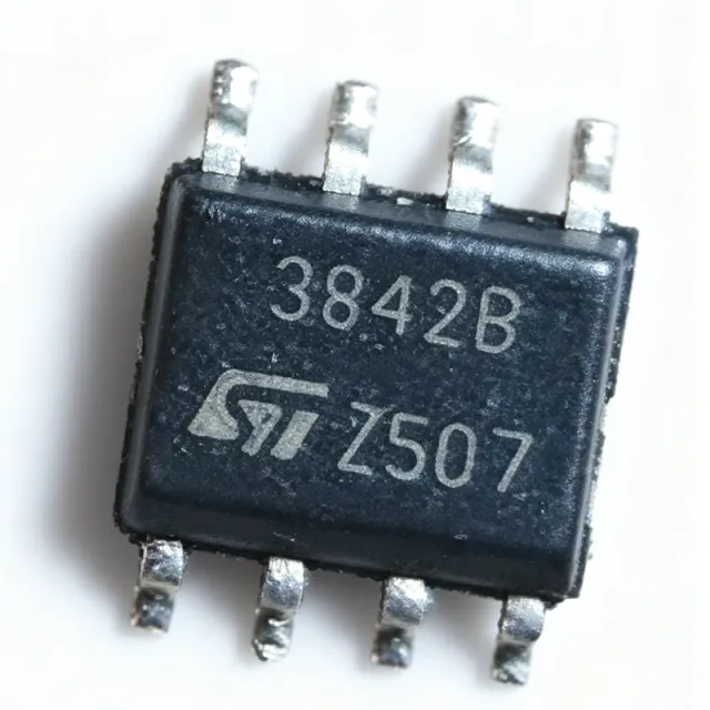
UC3842BD1 - Current Mode PWM Controller | STMicroelectronics | SMPS
The STMicroelectronics UC3842BD1 is a high-performance current-mode PWM controller designed for off-line and DC-to-DC converter applications. It operates with an input voltage range of 7.5V to 30V and provides a 1A peak output current for driving power MOSFETs. The device is available in an SOIC-8 package, making it suitable for compact power supply designs. A current-mode PWM controller is a type of switching regulator control IC that regulates output voltage by comparing the output error signal with a current-sense signal from the power switch. This architecture provides inherent feed-forward compensation, cycle-by-cycle current limiting, and simplified loop compensation compared to voltage-mode controllers. The UC3842BD1 belongs to the UC3842 family of PWM controllers, which are widely used in AC-DC adapters, battery chargers, and industrial power supplies. Key features of the UC3842BD1 include a trimmed oscillator for precise frequency control, an under-voltage lockout (UVLO) with hysteresis, a 5V reference output, and a high-gain error amplifier. The oscillator frequency is programmable up to 500 kHz, allowing designers to optimize transformer size and efficiency. The device also features a low startup current of 0.5 mA, which is critical for efficient power-up in battery-powered systems. The UC3842BD1 uses a fixed-frequency current-mode architecture with a maximum duty cycle of 96%. The error amplifier has a bandwidth of 1 MHz, enabling fast transient response. The current-sense comparator has a threshold of 1V, providing accurate cycle-by-cycle current limiting. The device is designed to operate over a junction temperature range of -40°C to +150°C, ensuring reliability in harsh environments. Typical applications include switch-mode power supplies (SMPS) for consumer electronics, industrial power converters, and battery chargers. The UC3842BD1 is also used in flyback and boost converter topologies, where its current-mode control simplifies loop compensation and improves line regulation. When designing with the UC3842BD1, ensure that the current-sense resistor is placed close to the IC to minimize parasitic inductance. The oscillator timing resistor and capacitor should be located near the RT/CT pin to reduce noise coupling. Proper grounding and decoupling of the VCC pin are essential for stable operation. This page synthesizes distributor pricing, drop-in alternatives, and practical design notes not found in the STMicroelectronics datasheet, providing engineers with a comprehensive resource for selecting and implementing the UC3842BD1.

UC3842BD1013TR - Current Mode PWM Controller | STMicroelectronics
The UC3842BD1013TR is a high-performance current-mode PWM controller from STMicroelectronics, designed for off-line and DC-to-DC converter applications. It operates as a boost or flyback regulator with isolation capability, providing a cost-effective solution for power supply designs. The device is housed in an 8-SOIC package and supports a switching frequency up to 500 kHz, with a peak output current of 1 A. Its input voltage is rated at 15 V, and it operates over a temperature range of 0°C to 70°C. A current-mode PWM controller is a type of switching regulator controller that uses the inductor current as a feedback signal to modulate the duty cycle of the output switch. This architecture provides inherent cycle-by-cycle current limiting, improved transient response, and simplified loop compensation compared to voltage-mode controllers. The UC3842BD1013TR belongs to the UC3842 family, which is widely used in AC-DC adapters, battery chargers, and isolated DC-DC converters. Key features of the UC3842BD1013TR include a trimmed oscillator for precise frequency control, current-mode operation up to 500 kHz, automatic feed-forward compensation, latching PWM for cycle-by-cycle current limiting, and an internally trimmed reference. These features enable stable and reliable operation in demanding power conversion applications. The device also includes under-voltage lockout (UVLO) and a totem-pole output stage capable of sourcing and sinking 1 A peak current to drive power MOSFET gates directly. Technically, the UC3842BD1013TR integrates a 5V reference, an error amplifier, a current-sense comparator, and a PWM latch. The oscillator frequency is set by an external resistor and capacitor, allowing designers to program the switching frequency from 50 kHz to 500 kHz. The current-sense input provides overcurrent protection by comparing the sensed voltage to a 1V threshold. The device's low startup current and low operating current contribute to high efficiency in power supplies. Typical applications include switch-mode power supplies (SMPS) for consumer electronics, industrial power converters, and isolated flyback converters for telecom and networking equipment. The UC3842BD1013TR is particularly suited for designs requiring a simple, reliable current-mode controller with minimal external components. When designing with this controller, ensure proper PCB layout to minimize noise on the current-sense and feedback paths. Use a low-ESR capacitor on the VCC pin and place the timing components close to the IC. Adequate thermal relief on the SOIC package is recommended for high-power applications.
UCC20225QNPLRQ1 - Automotive 4A/6A Dual Isolated Gate Driver | TI
The Texas Instruments UCC20225QNPLRQ1 is an automotive-grade (AEC-Q100 qualified) isolated single-input, dual-output gate driver with 4-A source and 6-A sink peak current, housed in a 13-pin VLGA (NPL) 5-mm x 5-mm package. It is designed to drive power transistors up to 5-MHz with best-in-class propagation delay and pulse-width distortion, and provides a 2.5-kV RMS reinforced isolation barrier between the input side and the two output drivers. A gate driver is a power amplifier that accepts a low-power logic-level PWM command from a controller and produces the high-current drive signal required to switch a power MOSFET, IGBT, or GaN/SiC transistor. Isolated gate drivers add a galvanic isolation barrier between the low-voltage control domain and the high-voltage power domain, protecting the controller and meeting safety creepage/clearance requirements in high-voltage systems. The UCC20225QNPLRQ1 sits inside the broader hierarchy of gate driver -> power management IC -> semiconductor, and is specifically tuned for high-side/low-side or half-bridge topologies with a single PWM input. Key features include 4-A source / 6-A sink peak drive, 30-ns typical propagation delay, 5-ns maximum channel-to-channel delay matching, minimum 100-V/ns common-mode transient immunity (CMTI), and an 8-V undervoltage lockout (UVLO) optimized for automotive 48-V systems. The VLGA-13 footprint occupies only 25 mm^2 of board area, enabling compact half-bridge and bootstrap designs in tight enclosures. The architecture combines a single CMOS/digital input with two independently isolated output channels, each capable of sinking/sourcing gate charge at MHz switching speeds. An integrated dead-time control feature and the 8-V UVLO threshold make this part particularly well-suited to automotive 48-V traction, OBC, and DC-DC converter stages using GaN or Si MOSFETs that need tight threshold management to prevent partial turn-on. Typical applications include 48-V mild-hybrid DC-DC converters, traction inverter gate-drive stages, on-board chargers (OBC), and isolated half-bridge power stages for industrial motor drives. Its 8-V UVLO specifically targets the 12-V class gate-drive rails common in 48-V automotive systems. When designing with this driver, place the bootstrap diode and capacitor directly adjacent to the high-side output pins to minimize parasitic inductance; insufficient decoupling on VDD can couple switching noise back into the logic input and cause spurious UVLO events at high dV/dt. This page synthesizes distributor pricing, drop-in alternatives, automotive 48-V application notes, and pin-by-pin design considerations beyond the manufacturer datasheet summary, helping power engineers accelerate ISO 26262-compliant design reviews.

UCC21520 - 4A/6A 5.7kVRMS Isolated Dual Gate Driver | TI
The Texas Instruments UCC21520 is an isolated dual-channel gate driver delivering 4-A source and 6-A sink peak output current, engineered to drive power MOSFETs, IGBTs, and SiC MOSFETs at switching frequencies up to 5 MHz with 5.7-kVRMS reinforced isolation in a 16-pin SOIC (DW) package. An isolated gate driver is an IC that combines galvanic isolation and signal amplification between a low-voltage controller and high-voltage power switches. Within the power management IC hierarchy, it sits between logic-level drivers and full gate-drive optocoupler solutions, enabling safe control of high-side and low-side switches in half-bridge, full-bridge, and LLC topologies. Key features include a wide VDD range of 6.5V to 25V, TTL/CMOS-compatible input thresholds, a DIS disable pin for output control, and UVLO protection on all supply pins. The device achieves a 19-ns propagation delay and 6-ns pulse-width distortion, best-in-class figures that preserve PWM accuracy at high switching frequencies. Technically, the UCC21520 uses TI capacitive isolation technology providing 100 V/ns common-mode transient immunity (CMTI), which prevents false triggering from fast dv/dt switching edges typical of SiC and GaN power stages. Programmable dead time via resistor setting and interlock function prevent shoot-through in bridge configurations. Typical applications include solar inverters, motor drives, EV charging and on-board chargers, isolated DC-DC converters, and UPS power stages, where high peak current efficiently charges large gate capacitances. Design tip: provide tight VDDA/VDDB decoupling and minimize gate-loop parasitic inductance; PCB layout critically affects realized CMTI and gate ringing performance.
UCC21520Q-Q1 - 4A/6A 5.7kVRMS Isolated Dual Gate Driver | TI
The Texas Instruments UCC21520Q-Q1 is an AEC-Q100 qualified, isolated dual-channel gate driver delivering 4-A source and 6-A sink peak output current. It drives power MOSFETs, IGBTs, and SiC MOSFETs at switching frequencies up to 5 MHz, with a 5.7 kVRMS reinforced capacitive isolation barrier providing a minimum of 125 V/ns common-mode transient immunity (CMTI). The device comes in a 16-pin wide-body SOIC (DW) surface-mount package. An isolated gate driver is a power-management IC that transfers a low-voltage logic-level PWM signal across a galvanic isolation barrier to drive the gate of a power semiconductor floating at high voltage. Within the signal-chain hierarchy, it sits between the PWM controller or microcontroller and the power stage, combining the functions of a logic buffer, level shifter, and isolation barrier in a single device. Key features include best-in-class propagation delay and pulse-width distortion, TTL- and CMOS-compatible input thresholds on INA, INB, and DIS pins that are independent of VDD, under-voltage lockout (UVLO) protection on all supply pins, and flexible dual-input configuration that allows the device to fit half-bridge, full-bridge, and dual low-side or high-side topologies. The 8-V UVLO variant ensures gate-drive integrity with SiC MOSFETs that require higher gate-source thresholds. The capacitive isolation architecture uses an on-chip SiO2 barrier delivering reinforced isolation rated at 5.7 kVRMS, supporting functional safety requirements in automotive traction inverters, onboard chargers, and high-voltage servo drives. High CMTI tolerance allows reliable operation in the presence of fast dv/dt switching edges typical of GaN and SiC power stages. Typical applications include automotive traction inverters, 48 V and high-voltage DC-DC converters, onboard chargers, solar string inverters, and industrial motor drives using SiC or IGBT power modules. When designing, verify that the VDDA/VDDB UVLO threshold matches the gate-drive voltage requirements of the selected power switch, and keep the gate-drive loop inductance minimal with closely coupled return paths.
UCC21521 - 4A/6A 5.7kVrms Isolated Gate Driver | TI
The Texas Instruments UCC21521 is an isolated dual-channel gate driver with 4-A source and 6-A sink peak output current, designed to drive power MOSFETs, IGBTs, and SiC MOSFETs at switching frequencies up to 5 MHz. It provides a reinforced isolation barrier of 5.7-kV RMS with at least 100-V/ns common-mode transient immunity (CMTI) in a 16-pin SOIC (DW) package. An isolated gate driver is a power management IC that translates low-voltage control logic into the high gate-drive current required to switch power transistors while maintaining galvanic isolation between controller and power stage. Within the power electronics hierarchy it sits between PWM controllers (DSPs, microcontrollers) and the power semiconductors they control, and is essential for safety and noise immunity in high-voltage converters. Key features include 19-ns typical propagation delay, 10-ns minimum pulse width, 5-ns maximum delay matching, and 6-ns maximum pulse-width distortion. These timing parameters enable precise, synchronized switching that reduces switching losses and EMI. Programmable dead time prevents shoot-through in half-bridge configurations, and the DIS enable pin supports power sequencing and fault protection. The UCC21521 uses TI capacitive isolation technology delivering CMTI of at least 100 V/ns for reliable operation in high-dv/dt environments such as SiC-based converters. Input pins use TTL and CMOS-compatible thresholds, allowing direct interface with 3.3-V microcontrollers and DSPs. The universal architecture supports dual low-side, dual high-side, or half-bridge driver configurations, and the device operates from -40C to +125C. Typical applications include motor drives, solar inverters, EV onboard chargers, and isolated DC-DC converters, where the 4-A/6-A drive strength and 5-MHz capability suit SiC MOSFET and IGBT power stages. Design tip: place decoupling capacitors close to VCCI and VDDA/VDDB pins and minimize gate-loop parasitic inductance to achieve specified timing performance and avoid dv/dt-induced false triggering.
UCC21521ADW - 4A/6A 5.7kVrms Isolated Gate Driver | TI
The Texas Instruments UCC21521ADW is a 4-A source / 6-A sink dual-channel isolated gate driver with 5.7-kVRMS galvanic isolation, capacitive coupling, an enable pin, programmable dead time, and 8-V UVLO, housed in a 16-pin SOIC (DW) package. An isolated gate driver is a power management IC that translates low-voltage logic signals across a galvanic isolation barrier to drive the gate of a power semiconductor such as a MOSFET, SiC FET, or IGBT. Within the power-supply and motor-control hierarchy, it sits between the PWM controller or microcontroller and the power stage, providing both the high peak currents needed for fast switching and the reinforced isolation needed for safety and level shifting. Key features include the universal configuration supporting dual low-side, dual high-side, or half-bridge operation, fast 19-ns typical propagation delay, 10-ns minimum input pulse width, and 5-ns maximum interchannel delay matching. The 4-A/6-A asymmetric source/sink drive accelerates turn-off to reduce switching losses in hard-switched converters. A programmable dead-time feature prevents shoot-through in half-bridge topologies, and the enable pin allows global shutdown for fault handling. The device uses TI capacitive isolation technology with a 5700-Vrms working isolation rating and 8-V undervoltage lockout on the output-side supply to guarantee complete gate enhancement before operation. Operating temperature spans -40C to +125C, supporting industrial power conversion, motor drives, solar inverters, and on-board chargers. Typical applications include half-bridge and full-bridge stages in server and telecom power supplies, three-phase inverters in motor drives, and isolated DC-DC converters where fast, precisely matched gate drive improves efficiency. For design, ensure the output-side VDD meets the 8-V UVLO threshold with adequate local decoupling, and size the dead time for the target power switch. This page synthesizes distributor pricing, drop-in alternatives, and practical design notes not found in the manufacturer datasheet.
UCC21521ADWR - 5.7kVrms 4A/6A Isolated Gate Driver | TI
The Texas Instruments UCC21521ADWR is a reinforced isolated dual-channel gate driver delivering 4-A source and 6-A sink peak output current with a 5700-Vrms withstand isolation rating, housed in a 16-pin SOIC (DW) package. It features dual inputs with an enable pin, an 8-V UVLO option, and programmable dead time, and can be configured as a dual low-side driver, dual high-side driver, or half-bridge driver. An isolated gate driver is a power management IC that transfers control signals across a galvanic isolation barrier, allowing a controller on the low-voltage side to switch power transistors such as MOSFETs, IGBTs, and SiC or GaN devices connected to a high-voltage rail. Isolated gate drivers sit within the broader gate driver and power management IC hierarchy and are essential wherever the gate-referenced potential differs from the logic-referenced potential. Key differentiating specifications include the 5.7-kVRMS reinforced isolation rating per the capacitive isolation technology, the asymmetric 4-A source / 6-A sink drive strength that favors fast turn-off for switch protection, and a wide supply range with an 8-V UVLO threshold suited to SiC MOSFET gate driving. The enable pin supports system-level safety interlocks, and the dead-time control eases half-bridge design. Architecturally, the UCC21521 uses a capacitive isolation barrier with on-chip signal isolation across a silicon-dioxide dielectric, providing high CMTI performance for switching noise immunity. The two output channels share a common topology with independent inputs, supporting inverting or non-inverting configurations depending on the ordering variant and input polarity. Typical applications include motor drives and industrial inverters, solar string inverters and MPPT power stages, and on-board chargers or DC-DC power stages in industrial power systems. The 4-A/6-A drive strength matches medium-power SiC and IGBT modules where fast gate charge delivery reduces switching losses. Design consideration: verify the input-side supply (VCCI) logic threshold matches the MCU or DSP bank voltage, and route the high-voltage side with adequate creepage and clearance per the reinforced-isolation footprint of the DW-16 package. This page synthesizes verified distributor pricing, drop-in alternatives, and practical design notes not consolidated in the manufacturer datasheet alone.
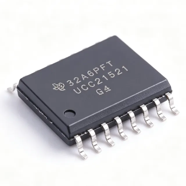
UCC21521DWR - 4A/6A 5.7kVrms Isolated Gate Driver | TI
The Texas Instruments UCC21521DWR is a 4-A source / 6-A sink dual-channel reinforced isolated gate driver with 5.7-kV RMS galvanic isolation, at least 100 V/ns common-mode transient immunity (CMTI), and a 16-pin SOIC (DW) package. An isolated gate driver is a power-management IC that translates low-voltage control logic from a microcontroller or DSP into the high peak current required to switch power transistors, while maintaining galvanic isolation between the control side and the power stage. Within the power-electronics hierarchy it sits between PWM controllers and MOSFETs, IGBTs, or SiC MOSFETs, and it is essential for safety isolation and noise immunity in high-voltage converters. Key features include 19-ns typical propagation delay, 5-ns maximum channel-to-channel matching, 6-ns maximum pulse-width distortion, and a 10-ns minimum input pulse width. These tight timing specifications reduce switching losses and minimize shoot-through risk. The DIS enable pin supports power sequencing and fast fault shutdown, and programmable dead time (for half-bridge configurations) prevents cross-conduction. Technically, the UCC21521 uses TI capacitive isolation technology to deliver the 5.7-kV RMS reinforced barrier with CMTI of at least 100 V/ns, making it robust in high dv/dt SiC environments. Input thresholds are TTL and CMOS compatible for direct 3.3-V logic interfacing, and an 8-V UVLO protects the power switch from under-driven operation. Typical applications include motor drives, solar string inverters, EV onboard chargers, and isolated DC-DC converters, where the 4-A/6-A drive strength and up-to-5-MHz switching capability suit SiC and IGBT power stages. Design tip: place decoupling capacitors directly at VCCI and VDDA/VDDB pins and minimize gate-loop inductance to achieve the datasheet timing figures and avoid dv/dt-induced false triggering. This page adds value beyond the datasheet with drop-in alternative comparisons, pricing tiers, and practical layout notes synthesized from distributor and manufacturer data.
UCC21521Q-Q1 - 4A/6A 5.7kVRMS Dual Gate Driver | Texas Instruments
The Texas Instruments UCC21521Q-Q1 is an AEC-Q100 qualified, 5.7-kVRMS isolated dual-channel gate driver delivering 4-A source and 6-A sink peak output current, housed in a 16-pin SOIC (DW) package. The device is universal in topology, supporting dual low-side, dual high-side, or half-bridge driver configurations, and includes an enable pin for system-level control. An isolated gate driver is a power management IC that provides galvanic isolation between the low-voltage controller side and the high-voltage power stage, allowing a microcontroller to safely drive power semiconductor switches such as MOSFETs, SiC FETs, and IGBTs. Gate drivers form the interface layer of the power-conversion hierarchy: controller -> signal isolator -> gate driver -> power switch. Key features include capacitive-coupled isolation rated at 5700 Vrms, high CMTI (common-mode transient immunity) for fast-switching wide-bandgap applications, a UVLO (undervoltage lockout) on both input and output supplies that prevents erratic gate drive during power-up, and an enable pin that places both outputs low for safety interlocks. The 4-A/6-A asymmetrical drive strength provides strong turn-off capability that minimizes switching losses and improves dv/dt immunity against parasitic turn-on. The Q1 grade guarantees operation from -40C to +125C ambient under AEC-Q100 automotive qualification, making the device suited to traction inverters, on-board chargers, and 48V systems. The universal channel configuration lets a single bill-of-material position cover half-bridge, dual low-side, and dual high-side designs, reducing qualification overhead across platforms. Typical applications include automotive traction inverters, OBC PFC and LLC power stages, DC fast-charger modules, solar string inverters, and industrial motor drives driving SiC or IGBT switches. The wide-body creepage and clearance of the SOIC-16 (DW) package supports reinforced isolation designs. Design consideration: size the gate-loop resistance to balance switching speed against ringing, and place the driver close to the power switch to minimize loop inductance; always verify CMTI margin against the fastest dv/dt in the system. Pricing data as of 2026-08-29; see tiers below for quantity pricing.

UCC21530 - 4A/6A 5.7kVRMS Isolated Dual Gate Driver | TI
The Texas Instruments UCC21530 is an isolated dual-channel gate driver delivering 4A source and 6A sink peak output current in a 14-pin SOIC (DWK) package. It is designed to drive IGBTs, Si MOSFETs, and SiC MOSFETs at switching frequencies up to 5MHz, with a 5.7kVRMS reinforced isolation barrier and a minimum common-mode transient immunity (CMTI) of 125V/ns. An isolated gate driver is a specialized power-management IC that provides galvanic isolation between a low-voltage controller (MCU or PWM controller) and a high-voltage power stage while supplying the peak current required to switch power transistors rapidly. It sits in the power electronics signal chain between the digital controller and the gate of an IGBT or MOSFET. The UCC21530 uses a capacitive isolation architecture, which enables high-speed signal transfer with low power consumption compared with optocoupler-based drivers. Key features include 4A/6A peak output current, 5.7kVRMS reinforced isolation, 125V/ns minimum CMTI, 3.3mm channel-to-channel spacing, an enable pin, and programmable dead time via the DT pin. According to the TI datasheet, the device offers best-in-class propagation delay and low pulse-width distortion, which reduces dead-time losses and enables precise, efficient switching. Undervoltage lockout (UVLO) on both the input and output sides adds system-level robustness. Architecturally, the UCC21530 comprises an input-side controller coupled through a capacitive isolation barrier to two secondary-side drivers. The reinforced barrier supports demanding safety standards, while internal functional isolation between the two outputs allows independent high-side and low-side operation in half-bridge and full-bridge configurations without external isolation components. Typical applications include three-phase motor drives, solar string inverters, EV onboard chargers, UPS systems, and server power supplies. High peak current and low propagation delay minimize switching losses, while high CMTI prevents false gate triggering at rapidly slewing switch nodes in SiC designs. When designing with the UCC21530, minimize gate-loop parasitic inductance, set dead time correctly via the DT pin to prevent shoot-through, and verify UVLO thresholds against your rail-sequencing plan for reliable startup. Pricing as of 2026-08-30 is available from authorized distributors listed in data sources.

UCC21530DWKR - 4A/6A Dual-Channel Isolated Gate Driver | TI
The Texas Instruments UCC21530DWKR is a 4A source / 6A sink, 5.7 kVRMS reinforced-isolated dual-channel gate driver in a 14-pin SOIC (DWK) package with 3.3 mm channel-to-channel spacing. It is engineered to drive IGBTs, silicon MOSFETs, and SiC MOSFETs up to 5 MHz switching frequency, with a minimum 125 V/ns common-mode transient immunity (CMTI) rating. A galvanically isolated gate driver is a power-semiconductor interface IC that translates low-voltage PWM control signals from a digital controller (MCU, DSP, or FPGA) into the high-voltage, high-current drive required to switch the gate of a power transistor. It belongs to the broader hierarchy of gate driver -> power management IC -> signal conditioning -> power conversion. Reinforced isolation, defined by IEC 60747-17, provides a 5.7 kVRMS working voltage plus transient overvoltage protection between the low-voltage primary side and the high-voltage secondary side, eliminating the need for optocouplers or external bootstrap circuits in many topologies. Key features include 4 A peak source / 6 A peak sink drive capability, 5.7 kVRMS reinforced isolation per UL 1577, 8 V to 18 V VDD supply range (VDDA/VDDB up to 25 V), programmable dead-time control via the DT pin, an enable pin for simultaneous shutdown of both outputs, internal functional isolation between the two secondary sides, and an extended -40C to +125C operating temperature range. The wide drive-voltage capability supports SiC MOSFET turn-on enhancement and IGBT gate-charge requirements across many power classes. The device employs TI's capacitive isolation technology using an internal SiO2 dielectric barrier, achieving CMTI of at least 125 V/ns and supporting switching frequencies up to 5 MHz. Fail-safe logic ensures that primary-side faults force both outputs LOW, preventing catastrophic half-bridge shoot-through conditions in motor drive and inverter applications. Typical applications include solar inverters, industrial motor drives (AC induction, BLDC, PMSM), telecom DC/DC converters using DAB/PSFB topologies, EV charging stations (OBC and DC fast charge), SiC FET-based high-frequency converters, and Class D audio amplifiers. The reinforced isolation barrier also allows direct drive of 600 V / 1200 V / 1700 V class power stages without additional isolation. When designing with the UCC21530DWKR, choose decoupling capacitors of at least 1 uF low-ESR ceramic on each VDD rail placed within 5 mm of the IC pins. The DT pin resistor sets dead time and must be selected based on the specific power-switch turn-off delay to prevent cross-conduction; consult the datasheet's dead-time programming section for the recommended resistor range. This page synthesizes distributor pricing, parametric drop-in alternatives, and practical PCB layout notes not consolidated on the manufacturer datasheet front page, providing engineers with a single decision-ready reference.

UCC21530Q-Q1 - 4A/6A 5.7kVRMS Isolated Gate Driver | TI
The Texas Instruments UCC21530Q-Q1 is an AEC-Q100 qualified, reinforced isolated dual-channel gate driver delivering 4A source and 6A sink peak output current, designed to drive IGBTs, Si MOSFETs, and SiC MOSFETs at switching frequencies up to 5MHz. It comes in a 14-pin SOIC (DWK) package with a 5.7kVRMS reinforced isolation barrier providing 3.3mm channel-to-channel spacing. An isolated gate driver is a power management IC that transfers logic-level PWM control signals across a galvanic isolation barrier to drive the gate of a high-side or low-side power switch floating at high voltage. Within the power-electronics hierarchy (gate driver -> isolated driver IC -> power management IC -> semiconductor), the UCC21530-Q1 occupies the critical interface between a microcontroller such as the TMS320F28004x C2000 family and the power stage. Key features include best-in-class propagation delay and pulse-width distortion, programmable dead time via a single DT pin resistor, a common-mode transient immunity (CMTI) of at least 125V/ns for operation on fast-switching GaN and SiC bridges, and TTL/CMOS-compatible input thresholds independent of the VDDI supply. An enable pin allows global shutdown, and both outputs can be interlocked for half-bridge configurations. The capacitive isolation architecture supports a maximum repetitive peak isolation voltage suitable for 800V-class automotive systems such as on-board chargers and traction inverters, though designers should verify creepage requirements against the 3mm package spacing. Wide VDDI operation on the output side accommodates 5V-to-20V gate-drive rails needed for SiC MOSFETs. Typical applications include automotive traction inverters, 800V on-board chargers (OBC), DC-DC converters, motor drives, and solar inverters. Pairing the driver with SiC MOSFETs such as the LMG3422 GaFET ecosystem or discrete SiC switches yields low-loss, high-frequency power stages. Design tip: size the DT-pin resistor precisely to set dead time, and place a low-ESR decoupling network (1uF plus 100nF) directly at VDDA and VDDB to sustain 4A/6A peak gate currents without droop.
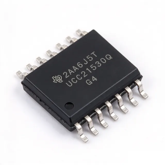
UCC21530QDWKRQ1 - 4A/6A 5.7kVrms Isolated Gate Driver | TI
The Texas Instruments UCC21530QDWKRQ1 is an automotive-grade, 4-A source / 6-A sink, 5.7-kVRMS reinforced isolated dual-channel gate driver with enable and programmable deadtime, housed in a 14-pin DWK (SOIC-14 wide-body) package. It drives IGBTs, SiC MOSFETs, and GaN power switches up to 5 MHz with best-in-class propagation delay (33 ns typical) and pulse-width distortion. The reinforced isolation barrier is rated to 5.7 kVRMS with a minimum 8.5-mm creepage / clearance and 3.3-mm channel-to-channel spacing, simplifying UL 1577 and IEC 60747-17 compliance for high-voltage systems. An isolated gate driver is a switching power-supply sub-system that translates low-side logic-level PWM into a high-voltage, floating gate-drive signal referenced to the switched-node of a half-bridge. It belongs to the gate-driver IC family, a category within power MOSFET/IGBT drivers, under the broader power management hierarchy. The UCC21530-Q1 integrates a silicon-oxide isolation transformer, two output channels (the chip itself), and is AEC-Q100-qualified for automotive environments by design. Key features include 4-A peak source and 6-A peak sink output current, a wide 18-V to 25-V VDD/VDDA range (3-V to 18-V on logic side), 33-ns typical propagation delay, 5-ns maximum channel-to-channel delay matching, 100-V/ns CMTI, and integrated programmable deadtime (DT) for shoot-through prevention. An active-low enable pin and a fault-ready open-drain output support sequencing and desaturation monitoring in three-phase inverters and PFC stages. Typical applications include traction inverters for EV powertrains, on-board chargers (OBC), industrial servo drives, solar string inverters, telecom DC/DC converters, and any 400-V / 800-V bus half-bridge topology requiring reinforced isolation. The DWK wide-body SOIC package provides 8.5 mm of creepage for high-voltage pollution-degree-2 environments. When designing with the UCC21530-Q1, place 1-uF / 100-nF decoupling on VDD/VDDA/VCCI close to the IC pins. Use a bootstrap diode + capacitor on the high-side channel whose voltage rating is rated for the DC bus plus transient ringing. Always respect the absolute-maximum VDD/VDDA of 30 V to avoid catastrophic gate-oxide damage. This page synthesizes distributor pricing, drop-in alternatives, and practical design notes not consolidated in the manufacturer datasheet — including same-package TI options, cross-brand validation notes, and BOM-optimization guidance unavailable on DigiKey/Mouser product pages.
UCC21540 - 4A/6A 5.7kVRMS Isolated Gate Driver | Texas Instruments
The Texas Instruments UCC21540 is a reinforced isolated dual-channel gate driver delivering up to 4-A peak source and 6-A peak sink current to drive power MOSFETs, IGBTs, and GaN transistors. It carries a 5.7-kVRMS galvanic isolation rating, and the DWK package option provides 3.3-mm channel-to-channel spacing for high bus-voltage industrial designs. An isolated gate driver is a specialized IC that provides galvanic isolation between a low-voltage controller and a high-voltage power stage, enabling safe, ground-loop-free switching of power transistors in the power-conversion hierarchy: gate driver -> isolated driver -> power management IC. The UCC21540 belongs to the UCC2154x family within TI's broad isolated gate driver portfolio, optimized for 10-12V driven MOSFETs and IGBTs. Key features include 4-A/6-A peak drive strength, 5.7-kVRMS reinforced isolation per the capacitive isolation technology, a programmable-deadtime (DT) pin that prevents shoot-through in half-bridge configurations, a disable (DIS) pin for system-level fault shutdown, and an 8-V UVLO on the secondary-side supply. VDD on the output side operates from 6.5V to 18V, supporting both dual low-side and half-bridge topologies. Technically, the device uses TI capacitive isolation technology, delivering fast propagation delay, low channel-to-channel matching error, and high common-mode transient immunity (CMTI), which is essential when switching at high frequency across large dv/dt events such as GaN half-bridge transitions. The dual-input configuration accepts both PWM-style inverting/non-inverting inputs for flexible control interfacing. Typical applications include server and telecom power supplies, industrial motor drives, solar string inverters, and EV onboard chargers, where its combination of drive strength, deadtime control, and isolation robustness maximizes converter efficiency and reliability. Design tip: keep the gate-drive loop compact, set the DT pin resistor for the deadtime your switches require, and respect creepage/clearance spacing on the PCB. According to TI, pricing and availability as of 2026-08-30.
UCC21540ADWR - 4A/6A Dual Isolated Gate Driver, 14-SOIC | TI
The Texas Instruments UCC21540ADWR is a 4A/6A dual-channel reinforced isolated gate driver with disable pin and programmable dead time, housed in a 14-pin SOIC (DW) package. The driver delivers 4A peak source and 6A peak sink current, supports up to 5.7kVrms galvanic isolation, and operates across an industry-standard 3V to 18V VCC range, making it suitable for driving power MOSFET, IGBT, and GaN transistors in half-bridge, dual low-side, or dual high-side configurations. An isolated gate driver is a semiconductor device that provides galvanic isolation between a low-voltage control circuit (such as a microcontroller or DSP) and a high-voltage power stage. By using capacitive or magnetic isolation barriers, these drivers protect low-voltage logic from high-voltage transients while delivering the high peak currents required to rapidly switch power FET gates. The UCC21540ADWR belongs to the isolated gate driver category, a sub-family of power management ICs that sits between MCU/DSP controllers and the discrete power switches in converters, motor drives, and solar inverters. Key features include 4A source / 6A sink peak drive current, 5.7kVrms basic isolation (per UL 1577), 1500Vrms working voltage, programmable dead time from 0 to several hundred nanoseconds via a single external resistor, and an active-low DISABLE pin for synchronized shutdown. The device supports up to 25V VDD supply for gate drive rails, and its dual-channel architecture permits independent control of high-side and low-side FETs in a half-bridge topology. The UCC21540ADWR uses TI's capacitive isolation technology with an integrated transformer driver on-chip, providing robust common-mode transient immunity (CMTI) and eliminating the need for optocouplers. The internal architecture includes a PWM input stage, oscillator, isolation barrier, and output buffer stages optimized for fast propagation delay (typically under 40ns) and minimal channel-to-channel skew, both critical for high-frequency switch-mode power supply designs. Typical applications include solar inverters, industrial motor drives, telecom brick converters, server and telecom power supplies, EV charging stations, and UPS systems. The wide VCC range also supports battery-powered portable equipment driving 12V to 48V bus rails. When designing with this part, observe that the disable pin (pin 6) defaults to a defined logic level - leave it tied high if unused. Dead-time programming resistor selection must be verified against the actual switching frequency, and a small bypass capacitor (typically 1nF to 10nF) is recommended near VCC and VDD supplies. This page synthesizes distributor pricing, drop-in alternatives (including same-family UCC21540DWK in the larger SOIC-16 DWK footprint), and practical design notes that complement the manufacturer datasheet.