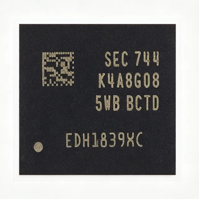
K4A8G085WB-BCTD - 8Gb DDR4 SDRAM 1Gx8 2666Mbps | Samsung
Teilenummer: K4A8G085WB-BCTD ✓ Aktiv| Menge | Stückpreis | Gesamt |
|---|---|---|
| 1 | $10.66 | $10,66 |
| 10 | $10.12 | $101,20 |
| 100 | $9.59 | $959,00 |
| 500 | $9.06 | $4.530,00 |
| 1.000 | $8.53 | $8.530,00 |
K4A8G085WB-BCTD Übersicht
DDR4 SDRAM (Double Data Rate 4 Synchronous Dynamic Random Access Memory) is the fourth generation of DDR DRAM, sitting within the memory hierarchy as the main-system-memory workhorse between cache memories and storage. Compared with DDR3, DDR4 lowers operating voltage from 1.5V to 1.2V, doubles bank groups, and raises prefetch efficiency, allowing higher densities and bandwidth per device.
Key features of the B-die include 8Gb density in a single die, x8 organization with differential DQS strobes, on-die termination (ODT), ZQ calibration, CRC and write CRC support, CA parity, and a wide operating temperature class per the -BCTD speed/temperature bin code. Samsung's B-die is famous in the enthusiast community for strong overclocking headroom thanks to its process characteristics.
Architecturally, the device uses a 16-bank / 4-bank-group structure with DDR4 burst lengths of 8 (BL8) and on-chip DLL for synchronized data capture. The asynchronous reset (RESET#) input protects against data corruption during power ramp, and dynamic ODT simplifies multi-rank routing.
Typical applications include embedded motherboards, networking and telecom line cards, industrial controllers, test equipment, and HPC memory modules (UDIMM/RDIMM/SODIMM designs).
Design consideration: DDR4 fly-by routing requires per-DQ write leveling and ZQ calibration resistor placement (240 ohm, 1%) close to the ZQ ball; controller timing (CL-tRCD-tRP per the speed bin) must match the firmware SPD settings.
This page synthesizes distributor pricing, verified drop-in alternatives, and practical DDR4 layout guidance not consolidated in the Samsung datasheet.
Drop-in-Alternativen für K4A8G085WB-BCTD – gleiches Gehäuse, Pin-kompatibel. Bauteile mit anderem Gehäuse, die eine PCB-Überarbeitung erfordern, sind ausgeschlossen.
Schnellvergleichstool – Wählen Sie Alternativbauteile für den Direktvergleich:
K4A8G085WC-BCTD
✓ Auf Lager
$50.85 / Stück
Datenblatt ansehen →K4A8G085WB-BCRC
✓ Auf Lager
$6.8 / Stück
Datenblatt ansehen →K4A8G085WB-BCPB
✓ Auf Lager
$13.7813 / Stück
Datenblatt ansehen →K4A8G085WG-BCWE
📋 Referenzalternative (nicht im Katalog)
K4A8G085WB-BCTD0
📋 Referenzalternative (nicht im Katalog)
K4A8G085WB-BCTD Grenzwerte & elektrische Eigenschaften
| Speichertyp | DDR4 SDRAM |
| Density | 8 Gb |
| Speicherorganisation | 1G x 8 |
| Datenrate | 2666 Mbps |
| Versorgungsspannung | 1.2 V |
| Die Revision | B-die |
| Gehäuse | FBGA-78 (78-ball TFBGA) |
| Montageart | Surface Mount |
| Bank Structure | 16 banks, 4 bank groups |
| Burst Length | BL8 |
| Termination | On-Die Termination (ODT), dynamic ODT |
| Eigenschaften | ZQ calibration, CRC, CA parity, asynchronous reset |
| Speed Bin | -BCTD (CL-tRCD-tRP bin) |
| Terminations | 78 |
| JEDEC-30 Package Code | R-PBGA-B78 |
K4A8G085WB-BCTD r-pbga-b78 Pinbelegungsleitfaden
Pinbelegung für K4A8G085WB-BCTD (r-pbga-b78-Gehäuse). Dieser digitale IC umfasst GPIO, Kommunikationsschnittstellen (UART, SPI, I2C) und Versorgungspins. Alternative Pin-Funktionen und Konfigurationsoptionen entnehmen Sie dem Herstellerdatenblatt. Unverzichtbar für Embedded-System-Design und PCB-Layout.

Keine detaillierten Pinbelegungsdaten verfügbar für K4A8G085WB-BCTD.
Siehe die Datenblatt für die vollständige Pin-Konfiguration.
Typische Anwendungen
K4A8G085WB-BCTD ist geeignet für 6 Anwendungs: Embedded Motherboards and Controllers, Networking and Telecom Line Cards, High-Performance Computing and Memory Modules, Industrial Automation and Machine Vision, Test and Measurement Equipment, Automotive-adjacent and Edge Computing Devices.
Embedded Motherboards and Controllers
The K4A8G085WB-BCTD fits embedded x86 and ARM motherboards that require 8Gb density in a compact 78-ball FBGA footprint. Its 1.2V supply keeps power budgets low relative to DDR3 solutions, and the asynchronous RESET# input protects memory contents during board-level power sequencing. In a single-chip-down (1Gx8) configuration, one device provides 1GB of main memory; two devices in a 64-bit bus provide 2GB with ranks configured for interleaving. The B-die's timing margin supports embedded controllers running at conservative 2133/2400 Mbps settings while retaining headroom for firmware tuning. On-die termination reduces external VTT termination component count on two-layer-capable embedded designs, and ZQ calibration keeps output impedance accurate across temperature.
Empfohlen
Networking and Telecom Line Cards
Network switches, routers, and telecom line cards use DDR4 for packet buffers, lookup tables, and control-plane memory. The K4A8G085WB-BCTD's 2666 Mbps data rate supplies roughly 2.6 GB/s peak bandwidth per 8-bit device, and its 4-bank-group architecture improves effective bandwidth under random access patterns typical of packet processing. CRC and CA parity features on this Samsung B-die detect command/address corruption on high-utilization backplanes, an important reliability feature for always-on telecom equipment. Multiple devices can be arranged in fly-by topology across ranks; dynamic ODT adjusts termination between writes without controller intervention, simplifying signal integrity at these data rates on dense line-card layouts.
Empfohlen
High-Performance Computing and Memory Modules
Samsung's B-die is the silicon of choice for enthusiast and workstation UDIMM/RDIMM/SODIMM builds because of its documented frequency and timing headroom. The K4A8G085WB-BCTD delivers 8Gb per chip, so a 16-chip unbuffered DIMM reaches 16GB, and the x8 organization supports ECC on x72 module configurations. Module designers value the BCTD bin's 2666 Mbps guaranteed operating point together with headroom toward 3200 Mbps-class timings. SPD EEPROM (per JEDEC module practice) programs the exact CL-tRCD-tRP bin for the host BIOS. CRC and ZQ calibration functions comply with standard DDR4 module reference designs, allowing direct integration into existing DIMM PCB stacks without modification.
Empfohlen
Industrial Automation and Machine Vision
Industrial PCs, PLCs, and machine-vision frame grabbers need reliable high-bandwidth memory for image buffers and control loops. The K4A8G085WB-BCTD's 1.2V operation reduces heat inside sealed fanless enclosures - important because DRAM refresh and reliability degrade at high junction temperatures. Its 8Gb density supports multiple 4K image frame buffers in vision pipelines, while the 2666 Mbps rate sustains streaming throughput from GigE/USB3 vision sensors. The device's asynchronous RESET# and CRC/CA parity improve fault behavior under noisy factory EMI conditions. For vibration-prone deployments, the lead-free FBGA package's small die-to-ball geometry provides better mechanical robustness than TSOP-era DDR packaging.
Empfohlen
Test and Measurement Equipment
Oscilloscopes, logic analyzers, and signal generators use large DRAM buffers for waveform capture. The K4A8G085WB-BCTD provides 1GB per device at 2666 Mbps, giving roughly 2.6 GB/s of streaming bandwidth per channel - adequate for sustained acquisition-to-memory transfers when organized in 64-bit-wide arrays. The B-die's timing margin lets instrument designers operate at conservative speeds for maximum noise margin while retaining the option of faster firmware settings in later product tiers. ZQ calibration maintains output impedance accuracy across the instrument's warm-up temperature drift, and the 78-ball FBGA's controlled ball layout eases length-matched routing on the high-layer-count PCBs typical of bench instruments.
Empfohlen
Automotive-adjacent and Edge Computing Devices
Edge AI gateways, smart-camera NVRs, and in-cabin infotainment platforms use DDR4 DRAM for model execution and video buffering. The K4A8G085WB-BCTD's 8Gb density supports convolutional-neural-network working sets of hundreds of megabytes with headroom, while its 2666 Mbps rate feeds embedded SoC memory controllers rated at DDR4-2666. The 1.2V rail simplifies integration with low-voltage PMICs common in these designs. CRC, CA parity, and dynamic ODT preserve data integrity in electrically noisy vehicle-adjacent environments. Note that this commercial-grade part is not AEC-Q100 qualified; industrial and consumer edge applications are appropriate, while true automotive powertrain use requires Samsung's automotive DDR4 lines.
Empfohlen
Zusammenfassung der empfohlenen Produkte
Technische Referenzdaten für K4A8G085WB-BCTD – Vergleich, Designhinweise und Compliance-Informationen.
Auswahlhilfe
Vergleich mit Alternativen
| Parameter | Dieses Produkt | K4A8G085WC-BCTD | K4A8G085WB-BCRC | K4A8G085WB-BCPB | K4A8G085WG-BCWE | K4A8G085WB-BCTD0 |
|---|---|---|---|---|---|---|
| Brand | Samsung Electronics | Samsung Electronics | Samsung Electronics | Samsung Electronics | Samsung Electronics | Samsung Electronics |
| Package | FBGA-78 | FBGA-78 - same | FBGA-78 - same | FBGA-78 - same | FBGA-78 - same | FBGA-78 (TFBGA) - same |
| Density | 8 Gb | 8 Gb | 8 Gb | 8 Gb | 8 Gb | 8 Gb |
| Organization | 1G x 8 | 1G x 8 | 1G x 8 | 1G x 8 | 1G x 8 | 1G x 8 |
| Data Rate | 2666 Mbps | 2666 Mbps | 2400 Mbps | 2400 Mbps | 3200 Mbps | 2666 Mbps |
| Supply Voltage | 1.2 V | 1.2 V | 1.2 V | 1.2 V | 1.2 V | 1.2 V |
| Die Revision | B-die | C-die | B-die | B-die | G-die family | B-die |
Wichtigste Unterscheidungsmerkmale
- Highest documented timing headroom in Samsung 8Gb DDR4 family (vs. K4A8G085WC-BCTD)
- 2666 Mbps guaranteed bin over BCRC/BCPB variants (vs. K4A8G085WB-BCRC)
- Cost advantage over equivalent-availability listings (vs. K4A8G085WC-BCTD)
Designhinweise
Route DDR4 address/command/control lines in fly-by topology from the controller through each DRAM to the end of the chain, with per-device length taper. DQ/DQS/DM signals route point-to-point in matched groups with length matching to +/-10 mils intra-group (x8 parts need one DQS pair per byte lane). Reference all signal layers to solid ground planes; keep DDR4 signals off board edges and away from switching regulator inductors. Place series damping resistors only if the controller's design guide requires them - modern DDR4 usually relies on ODT and controller drive strength instead.
Provide a clean 1.2V VDD rail with bulk capacitance plus 0.1uF and 0.01uF ceramics distributed across the DRAM power balls. Generate VREFCA and VREFDQ from a precision DDR4 VDDQ-tracking reference (e.g., a dedicated reference generator) rather than a simple resistor divider when VDD noise exceeds a few millivolts. Estimated: at 2666 Mbps with moderate utilization, per-device current is on the order of hundreds of milliamps - size the VRM per the Samsung/current-calculated IDD figures in the datasheet and your controller's power tool. Place a single 240 ohm 1% resistor from ZQ to GND, as short as possible.
Do not mix speed bins in the same rank/byte lane without validating the weakest-bin timing in firmware - a 2400 Mbps -BCRC part installed in a 2666 Mbps -BCTD socket will fail margin tests if SPD settings assume 2666. RESET# must be asserted low during power ramp per the DDR4 power-ramp sequence, or data corruption and excess current can occur. After any die-revision substitution (B-die to C-die), rerun full read/write margin and training validation - pin compatibility does not guarantee identical timing windows at every operating point.
Compliance-Informationen
RoHS/REACH status not stated in the retrieved web data; verify on the Samsung product page. Not an AEC-Q100 automotive part - this is a commercial/industrial DDR4 component.


