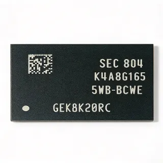
K4AAG165WB-MCRC - 16Gb DDR4 SDRAM, 2400 Mbps | Samsung
Teilenummer: K4AAG165WB-MCRC ✓ Aktiv| Menge | Stückpreis | Gesamt |
|---|---|---|
| 1 | $9.16 | $9,16 |
| 10 | $8.7 | $87,00 |
| 100 | $8.24 | $824,00 |
| 500 | $7.82 | $3.910,00 |
| 1.000 | $7.42 | $7.420,00 |
K4AAG165WB-MCRC Übersicht
DDR4 SDRAM (Double Data Rate 4 Synchronous Dynamic Random Access Memory) is the fourth generation of the JEDEC-defined DDR memory family. In the system hierarchy, DRAM sits below CPU caches as the primary working memory, bridging the speed gap between processors and storage. DDR4 improved on DDR3 by lowering the operating voltage from 1.5 V to 1.2 V, doubling bank groups, and raising data rates up to 3200 Mbps and beyond.
Key features of the K4AAG165WB-MCRC include its 16 Gb density in a single x16 organization, 2400 Mbps data rate for approximately 19.2 GB/s of peak bandwidth per chip at DDR4-2400, and the low 1.2 V core supply that reduces power consumption versus DDR3 alternatives. The x16 organization simplifies memory-down designs by requiring fewer chips than x8 parts for a given bus width, and the compact 96FBGA footprint keeps routing short for signal integrity at 1200 MHz clock rates.
The WB-generation die uses Samsung advanced DRAM process technology with bank-group architecture that allows faster sequential access within a burst. On-die termination (ODT), DLL-off mode, and programmable CAS latency support board-level timing optimization. The part supports standard DDR4 commands including ACT, PRE, REF, and MRS via mode registers, and the 96-ball FBGA ball map follows the JEDEC-standard x16 DDR4 footprint, enabling second-source drop-in compatibility with other JEDEC-compliant 16 Gb x16 DDR4 components.
Typical applications include laptop and notebook main memory (memory-down soldered DRAM), embedded industrial computing, networking appliances, set-top boxes, and edge AI inference boards where 2 GB per chip and x16 bus organization are required. It is widely used as a replaceable soldered DRAM on consumer laptop motherboards.
When designing with this part, follow DDR4 routing guidelines: length-match the 16 data bits per byte-lane, implement VTT termination, and decouple the 1.2 V VDD rail with at least 10 uF plus 0.1 uF per device. Verify controller MRS programming matches the -M (2400 Mbps, CL17-class) speed bin.
This page synthesizes distributor pricing, pin-compatible drop-in alternatives across Samsung and Micron, and practical design notes not found in the manufacturer datasheet.
Drop-in-Alternativen für K4AAG165WB-MCRC – gleiches Gehäuse, Pin-kompatibel. Bauteile mit anderem Gehäuse, die eine PCB-Überarbeitung erfordern, sind ausgeschlossen.
Varianten dieser Serie
Modelle derselben Serie, die drop-in-kompatibel sind mit K4AAG165WB-MCRC (gleiche Bauform und Footprint) – abweichend in Data Rate, Package, Clock Frequency, Interface, Memory Size.
Schnellvergleichstool – Wählen Sie Alternativbauteile für den Direktvergleich:
K4AAG165WB-MCTD
✅ Drop-In📋 Referenzalternative (nicht im Katalog)
K4AAG165WB-MCRC0CV
✅ Drop-In📋 Referenzalternative (nicht im Katalog)
K4AAG165WB-BCWE
✅ Drop-In📋 Referenzalternative (nicht im Katalog)
K4AAG165WB-MCPB
✅ Drop-In📋 Referenzalternative (nicht im Katalog)
K4AAG165WA-BCTD
✅ Drop-In✓ Auf Lager
$60.59 / Stück
Datenblatt ansehen →MT40A256M16GE-075E:B
✅ Drop-In✓ Auf Lager
$3.95 / Stück
Datenblatt ansehen →K4AAG165WB-MCRC Grenzwerte & elektrische Eigenschaften
| Speichertyp | DDR4 SDRAM |
| Density | 16 Gb (2 GB) |
| Speicherorganisation | 1G x 16 |
| Datenrate | 2400 Mbps (DDR4-2400) |
| Versorgungsspannung | 1.2 V |
| Betriebstemperatur | 0 C to +85 C |
| Gehäuse | 96FBGA |
| Montageart | Surface Mount |
| Schnittstelle | Parallel, DDR4 |
| Bank Architecture | DDR4 bank-group architecture |
| Clock Frequency | 1200 MHz (DDR4-2400) |
| Peak Bandwidth (per device) | 19.2 GB/s (estimated: 2400 Mbps x 16 bits / 8) |
| RoHS-Status | Compliant (per LCSC/JLCPCB listing: FBGA-96 DRAM ROHS) |
K4AAG165WB-MCRC 96fbga Pinbelegungsleitfaden
Pinbelegung für K4AAG165WB-MCRC (96fbga-Gehäuse). Dieser digitale IC umfasst GPIO, Kommunikationsschnittstellen (UART, SPI, I2C) und Versorgungspins. Alternative Pin-Funktionen und Konfigurationsoptionen entnehmen Sie dem Herstellerdatenblatt. Unverzichtbar für Embedded-System-Design und PCB-Layout.

Keine detaillierten Pinbelegungsdaten verfügbar für K4AAG165WB-MCRC.
Siehe die Datenblatt für die vollständige Pin-Konfiguration.
Typische Anwendungen
K4AAG165WB-MCRC ist geeignet für 6 Anwendungs: Laptop / Notebook Main Memory (Memory-Down), Embedded Industrial Computing, Networking and Communication Equipment, Set-Top Box and Smart TV, Edge AI Inference Boards, Test and Measurement / Logic Analyzer Host Memory.
Laptop / Notebook Main Memory (Memory-Down)
The K4AAG165WB-MCRC is a dominant soldered-down DRAM choice for consumer laptop motherboards. Its 16 Gb (2 GB) capacity per chip lets a 64-bit design reach 8 GB with just four devices and 16 GB with eight, minimizing PCB area versus SODIMM modules. The 1.2 V DDR4 rail cuts memory subsystem power roughly 20% compared with DDR3 at 1.5 V, directly extending battery runtime. Placed on the JEDEC-standard x16 96FBGA footprint, the part supports drop-in substitution with K4AAG165WB-MCTD or Micron equivalents during repair and production second-sourcing. At 2400 Mbps per pin, a 64-bit four-chip bank delivers about 76.8 GB/s aggregate bandwidth, sufficient for mainstream CPU iGPU frame buffers and application memory. BGA rework with a proper stencil makes field repair practical.
Empfohlen
Embedded Industrial Computing
Industrial PCs, HMI panels, and edge gateways use the K4AAG165WB-MCRC as soldered system memory where vibration and temperature exclude socketed modules. The 96FBGA package withstands mechanical stress far better than DIMM connectors, and the 1.2 V rail reduces heat inside sealed fanless enclosures. Its 2 GB-per-chip density supports Linux/RTOS images with headroom for data logging, and the x16 organization matches the 16-bit or 32-bit memory controllers common on embedded SoCs from NXP, TI, and Rockchip. At 2400 Mbps the part supplies roughly 19.2 GB/s per device, adequate for protocol processing and local analytics. Designers should verify the 0 to 85 C commercial range against enclosure derating, or select an industrial temperature suffix variant for extended environments.
Empfohlen
Networking and Communication Equipment
Routers, switches, and NPUs use DDR4 for packet buffers, flow tables, and control-plane memory. The K4AAG165WB-MCRC's bank-group architecture sustains sequential bursts well suited to streaming packet data at line rate, and 2 GB per chip allows deep buffering in a small board area. A 32-bit or 64-bit x16 DDR4 controller bank using four to eight of these devices provides 8 to 16 GB of buffering with about 19.2 GB/s per device of bandwidth at 2400 Mbps. The 1.2 V supply keeps thermal budgets manageable in 1U appliances with limited airflow. Follow DDR4 fly-by or short-branch routing with per-byte length matching, and program controller ODT settings per Samsung datasheet recommendations to maintain signal integrity at 1200 MHz clock rates.
Empfohlen
Set-Top Box and Smart TV
Broadcast and streaming set-top boxes rely on the K4AAG165WB-MCRC for application, graphics, and video buffer memory. A single 16 Gb x16 chip provides 2 GB, which comfortably holds dual 4K video pipelines, UI frameworks, and middleware in cost-optimized designs. The 96FBGA footprint fits dense main-board layouts next to the SoC, shortening the DDR4 bus for reliable 2400 Mbps operation. The 1.2 V rail reduces standby and active power, supporting ENERGY STAR-class consumption targets. x16 organization matches the 16-bit and 32-bit DDR4 controllers typical of STB SoCs. Designers should budget refresh overhead and enable DDR4 self-refresh for fast standby resume, and verify SoC MRS programming against the MCRC speed bin.
Empfohlen
Edge AI Inference Boards
Edge AI modules for camera analytics and sensor fusion use the K4AAG165WB-MCRC to hold quantized model weights and activation buffers alongside the SoC. One 2 GB chip keeps small CNNs and feature pipelines resident without eMMC swap latency, and 19.2 GB/s per-device bandwidth at DDR4-2400 feeds NPU MAC arrays in compact SoCs. Soldered 96FBGA mounting survives shock and vibration in mobile robots and smart cameras, while the 1.2 V rail limits thermal load inside sealed camera housings. For vision workloads, a 32-bit dual-chip bus (4 GB, ~38.4 GB/s) is a common configuration. Verify the inference SoC supports the MCRC speed bin, and place devices symmetrically around the SoC for balanced fly-by routing.
Empfohlen
Test and Measurement / Logic Analyzer Host Memory
Bench instruments and logic analyzers capture deep waveform traces into DDR4, making the K4AAG165WB-MCRC's 2 GB-per-chip density valuable for long record lengths. Four x16 devices on a 64-bit bus store 8 GB of acquisition data with approximately 76.8 GB/s streaming bandwidth at 2400 Mbps, sufficient for sustained high-sample-rate capture into memory. The soldered 96FBGA package resists connector wear in bench environments, and the 0 to 85 C range covers typical lab conditions. FPGA-based memory controllers should implement DDR4 write-leveling and read-training per Samsung datasheet initialization sequences. Keep VTT termination and reference voltages tightly regulated; measurement instruments are sensitive to DDR4-induced jitter on shared power planes.
Empfohlen
Zusammenfassung der empfohlenen Produkte
Technische Referenzdaten für K4AAG165WB-MCRC – Vergleich, Designhinweise und Compliance-Informationen.
Auswahlhilfe
Vergleich mit Alternativen
| Parameter | Dieses Produkt | K4AAG165WB-MCTD | K4AAG165WB-MCRC0CV | K4AAG165WB-BCWE | K4AAG165WA-BCTD | MT40A256M16GE-075E:B |
|---|---|---|---|---|---|---|
| Package | 96FBGA | 96FBGA - same | 96FBGA - same | 96FBGA - same | 96FBGA - same | 96FBGA - same (JEDEC x16 ball map) |
| Brand | Samsung Electronics | Samsung Electronics | Samsung Electronics | Samsung Electronics | Samsung Electronics | Micron Technology |
| Density | 16 Gb (2 GB) | 16 Gb (2 GB) | 16 Gb (2 GB) | 16 Gb (2 GB) | 16 Gb (2 GB) | 16 Gb (2 GB) |
| Organization | 1G x 16 | 1G x 16 | 1G x 16 | 1G x 16 | 1G x 16 | 256M x 16 |
| Supply Voltage | 1.2 V | 1.2 V | 1.2 V | 1.2 V | 1.2 V | 1.2 V |
| RoHS | Compliant | Compliant | Compliant | Compliant | Compliant | Compliant |
Wichtigste Unterscheidungsmerkmale
- Lowest-cost standard speed bin (vs. K4AAG165WB-BCWE)
- Drop-in second sourcing within Samsung family (vs. K4AAG165WB-MCTD)
- Cross-brand JEDEC footprint compatibility (vs. MT40A256M16GE-075E:B)
Designhinweise
Follow DDR4 routing guidelines for the 96FBGA x16 device: length-match DQ0-15 to DQS within +/-25 mils (per-layer), keep the clock/strobe differential pairs tightly coupled, and use fly-by routing for multi-device buses with per-device decoupling. Place at least one 0.1 uF ceramic capacitor per VDD/VDDQ ball pair within 2 mm of the package, plus bulk 10 uF per rail. Connect all VSS balls to a solid ground plane with multiple vias to minimize return-path inductance at 1200 MHz data rates.
The K4AAG165WB-MCRC runs from a 1.2 V VDD/VDDQ rail. Estimate worst-case dynamic power per device at roughly 1 W (estimated: 2400 Mbps x 16 bits x typical DDR4 per-pin switching energy plus refresh baseline; verify against the Samsung datasheet IDD table for your access pattern). Budget VTT termination current separately - VTT can draw up to half the bus current on a loaded 64-bit bus. Use a dedicated DDR4 VTT LDO or switcher with at least 2 A capability per 64-bit bank and place sense points at the last device on the bus.
A frequent repair/rework failure is substituting a different speed bin without reprogramming the SoC memory controller. The MCRC suffix is a DDR4-2400, 0 to 85 C commercial bin; if you populate a K4AAG165WB-BCWE (3200 Mbps) the board generally works, but populating a slower bin than the controller expects causes training failures. Also, during BGA rework, profile the 96FBGA with a lead-free reflow ramp (peak ~245-250 C) and inspect with X-ray for shorts on the 0.5 mm-class ball pitch - hidden head-in-pillow defects are common with reused balls.
At 2400 Mbps, DDR4 write leveling and read training are mandatory. Enable the controller's ZQ calibration and program ODT values per the Samsung datasheet recommendation for a single-rank x16 configuration. For two-device fly-by buses, keep the trace stub from the series termination resistor under 100 mils and simulate eye diagrams at the far-end device. Excessive ISI shows up as marginal read margins during temperature cycling, so validate across the full 0 to 85 C range, not just room temperature.
Compliance-Informationen
RoHS compliance stated in LCSC/JLCPCB listing ('FBGA-96 DRAM ROHS'). Other compliance attributes not stated in provided data.