Samsung Electro-Mechanics

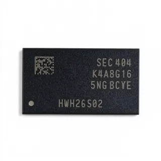
K6X0808C1D-GF70T00 - 256Kbit 32Kx8 Async SRAM 70ns | Samsung

Teilenummer: K6X0808C1D-GF70T00 ✓ Aktiv
Auf Lager Versand in 1–3 Werktagen
5 V Vdss 28-SOP Package Fully static, no clock or refresh required Speed SRAM - Asynchronous Memory
Ab $1.85 USD / Stück
MOQ: 1 |
Preis aktualisiert: 2026-09-01
Mengenpreise
Menge Stückpreis Gesamt
1 $3.2 $3,20
10 $2.85 $28,50
100 $2.45 $245,00
500 $2.1 $1.050,00
1.000 $1.85 $1.850,00
ℹ️ Alle Preise sind in USD

K6X0808C1D-GF70T00 Übersicht

The Samsung Semiconductor K6X0808C1D-GF70T00 is a 256Kbit asynchronous low-power CMOS static RAM organized as 32K x 8 bits, with a 70 ns access time, housed in a 28-pin SOP (small outline package) surface-mount case. It operates from a standard 5 V supply and communicates over a parallel address/data bus.

Static RAM (SRAM) is a type of volatile semiconductor memory that stores each bit in a bistable latch circuit, so data is retained as long as power is applied and no refresh cycles are required, unlike DRAM. Within the memory IC hierarchy, SRAM sits alongside DRAM, EEPROM and Flash as a solid-state memory family, and asynchronous SRAM specifically means accesses are controlled purely by address, chip-enable (CE), output-enable (OE) and write-enable (WE) pins with no external clock.

Key features include the fast 70 ns address access time, a fully static design requiring no clock or refresh, CMOS technology for low power consumption, and TTL-compatible I/O levels that simplify interfacing with legacy 5 V microcontrollers and microprocessors. The three control lines (CE, OE, WE) allow easy bus-mastering, bank selection and read/write gating in 8-bit systems.

Fabricated on Samsung's advanced CMOS process, the K6X0808C1D family supports various operating temperature ranges and multiple package types for system design flexibility, according to the manufacturer datasheet. The simple asynchronous interface keeps timing design straightforward: address setup, CE/OE access, and write pulse widths all fall within the 70 ns speed grade budget.

Typical applications include 5 V embedded controllers, industrial equipment retrofits and spare-part repairs, telecom line cards, test and measurement instruments, and buffer memory in legacy 8-bit and 16-bit microprocessor systems that use JEDEC-standard 32K x 8 SRAM footprints.

A key design consideration is power integrity: decouple the 5 V rail with a 0.1 uF ceramic capacitor close to pin 28, and ensure CE is actively driven because deselected standby current is far lower than active current. Avoid floating the control lines during power-up to prevent spurious writes.

This page adds unique value beyond the datasheet by consolidating drop-in alternatives, distributor pricing context, pinout, and practical design notes for sourcing and repair engineers.

Drop-in-Alternativen für K6X0808C1D-GF70T00 – gleiches Gehäuse, Pin-kompatibel. Bauteile mit anderem Gehäuse, die eine PCB-Überarbeitung erfordern, sind ausgeschlossen.

Varianten dieser Serie

Modelle derselben Serie, die drop-in-kompatibel sind mit K6X0808C1D-GF70T00 (gleiche Bauform und Footprint) – abweichend in Memory Type, Package, Data Bus Width, Access Time, Organization.

Samsung Electronics
Memory Type: Asynchronous SRAM
Access Time: 55 ns
Vergleichen mit K6X0808C1D-GF70T00 →
Samsung Electronics
Memory Type: Asynchronous SRAM (CMOS)
Package: 28-SOP (PDSO28)
Vergleichen mit K6X0808C1D-GF70T00 →
Samsung Electronics
Data Bus Width: 8 bit (I/O0-I/O7)
Vergleichen mit K6X0808C1D-GF70T00 →
Samsung Electro-Mechanics
Package: 28-SOP (450 mil)
Data Bus Width: 8 bit
Access Time: 55 ns
Vergleichen mit K6X0808C1D-GF70T00 →
Samsung Electro-Mechanics
Package: 28-SOP (450 mil)
Access Time: 55 ns
Vergleichen mit K6X0808C1D-GF70T00 →
Samsung Electronics
Data Bus Width: 8 bit (tri-state I/O)
Organization: 32K x 8 bit
Vergleichen mit K6X0808C1D-GF70T00 →

Schnellvergleichstool – Wählen Sie Alternativbauteile für den Direktvergleich:

K6X0808C1D-GF70000

✅ Drop-In
Samsung Electronics
📦 28-SOP
SRAM - Asynchronous · 256 Kbit · 32K x 8 bit · Parallel · 70 ns · 4.5 V · 5.5 V · Low Power CMOS

✓ Auf Lager

$1.1 / Stück

Datenblatt ansehen →

K6X0808C1D-GF55T00

✅ Drop-In
Samsung Electro-Mechanics
📦 28-SOP
SRAM - Asynchronous · 256 Kbit · 32K x 8 · 55 ns · Parallel · N/A (asynchronous) · CMOS

✓ Auf Lager

$1.05 / Stück

Datenblatt ansehen →

K6X0808C1D-BF70T

✅ Drop-In
Samsung Electronics
📦 28-SOP
SRAM - Asynchronous · 256 Kbit · 32K x 8 · Parallel · 70 ns · 70 ns · 4.5 V to 5.5 V · -40C to +85C (TA)

✓ Auf Lager

$1.05 / Stück

Datenblatt ansehen →

K6X0808C1D-BF55

✅ Drop-In
Samsung Electronics
📦 28-SOP
Asynchronous SRAM · 256 Kbit · 32K x 8 · 55 ns · Parallel · 5 V · CMOS · 28-SOP

✓ Auf Lager

$1.85 / Stück

Datenblatt ansehen →

IS62C256AL-70

✅ Drop-In
📦 28-SOP
cross-brand JEDEC 62256-class equivalent, 32K x 8, 5 V, 70 ns, pin-to-pin 28-SOP

📋 Referenzalternative (nicht im Katalog)

AS6C256-70SIN

✅ Drop-In
📦 28-SOP
cross-brand JEDEC 62256-class equivalent, 32K x 8, 5 V, 70 ns, same footprint

📋 Referenzalternative (nicht im Katalog)

K6X0808C1D-GF70T00 Technische Daten

Speichertyp SRAM - Asynchronous
Speichergröße 256 Kbit
Speicherorganisation 32K x 8
Access Time 70 ns
Schnittstelle Parallel
Technology CMOS
Versorgungsspannung 5 V
Montageart Surface Mount
Gehäuse 28-SOP
I/O Type Common Data I/O, TTL compatible
Control Signals CE, OE, WE
Clock / Refresh Fully static, no clock or refresh required
Packaging Tape & Reel (T00 suffix)

K6X0808C1D-GF70T00 Pin-Konfiguration

Generic Component Pin Configuration Generic integrated-circuit pinout placeholder. Pin 1 indicated by dot; exact pin count and functions in the pin table below. 1 N 2 N-1 3 N-2 4 N-3 Pin Configuration See pin table below for pin functions Package-specific diagram not available
Pin 1 A14 — Address input bit 14
Pin 2 A12 — Address input bit 12
Pin 3 A7 — Address input bit 7
Pin 4 A6 — Address input bit 6
Pin 5 A5 — Address input bit 5
Pin 6 A4 — Address input bit 4
Pin 7 A3 — Address input bit 3
Pin 8 A2 — Address input bit 2
Pin 9 A1 — Address input bit 1
Pin 10 A0 — Address input bit 0
Pin 11 I/O0 — Data input/output bit 0
Pin 12 I/O1 — Data input/output bit 1
Pin 13 I/O2 — Data input/output bit 2
Pin 14 GND — Ground
Pin 15 I/O3 — Data input/output bit 3
Pin 16 I/O4 — Data input/output bit 4
Pin 17 I/O5 — Data input/output bit 5
Pin 18 I/O6 — Data input/output bit 6
Pin 19 I/O7 — Data input/output bit 7
Pin 20 CE — Chip enable (active low)
Pin 21 A10 — Address input bit 10
Pin 22 OE — Output enable (active low)
Pin 23 A11 — Address input bit 11
Pin 24 A9 — Address input bit 9
Pin 25 A8 — Address input bit 8
Pin 26 A13 — Address input bit 13
Pin 27 WE — Write enable (active low)
Pin 28 VCC — Power supply, 5 V

Typische Anwendungen

K6X0808C1D-GF70T00 ist geeignet für 6 Anwendungs: Legacy 5V Embedded Controllers, Industrial Equipment Repair and Sustaining Engineering, Telecom Line Cards and Network Equipment, Test and Measurement Instruments, Battery-Backed Data Retention Modules, Retrofit and Upgrade of 8-bit Microprocessor Boards.

🔧

Legacy 5V Embedded Controllers

The K6X0808C1D-GF70T00 fits legacy 5 V microcontroller and microprocessor systems that use the JEDEC 62256-class 32K x 8 SRAM footprint. Its 70 ns access time comfortably supports 8 MHz-class bus timings, and TTL-compatible common I/O lines connect directly to processors such as the 8051, 68HC11, Z80 and early 16-bit MPUs without level shifting. Because the device is fully static, no refresh controller or bus arbitration logic is needed, preserving the original board design. The 28-SOP surface-mount package allows direct reflow onto existing land patterns during board repair or re-manufacture of legacy industrial and telecom controllers.

🏭

Industrial Equipment Repair and Sustaining Engineering

PLCs, motor drives, process controllers and CNC equipment from the 1990s and 2000s frequently used 5 V, 32K x 8 asynchronous SRAM such as the K6X0808C1D-GF70T00 for parameter and data storage. When these devices fail, the Samsung part restores form-fit-function without PCB modification. Its fully static CMOS design means the replacement simply drops into the 28-SOP socket or land pattern, and the 70 ns timing matches the original bus budget. Distributors including DigiKey Marketplace and Precision Logic stock the part specifically for repair quantities, making it a sustaining-engineering staple for factory maintenance teams extending machine life.

🌐

Telecom Line Cards and Network Equipment

Telecom line cards, channel banks and legacy transmission equipment commonly used 32K x 8 SRAM as frame buffers, lookup tables and configuration memory. The K6X0808C1D-GF70T00's 70 ns access time supports channel-sampled data buffering, while its low CMOS standby current keeps power budgets within card limits when memory banks are deselected via CE. The three-line control interface (CE, OE, WE) allows simple bank selection in multi-chip memory arrays typical of line-card designs. The 28-SOP package withstands standard reflow profiles, supporting card-level rework in network maintenance depots still servicing legacy T1/E1 and PBX hardware.

📊

Test and Measurement Instruments

Oscilloscopes, data loggers, bench power supplies and signal generators of the 5 V generation used asynchronous SRAM for waveform capture buffers and calibration storage. The K6X0808C1D-GF70T00's deterministic 70 ns access time provides consistent read latency across the full operating range, which matters for calibrated timing paths in instruments. Its 32K x 8 organization offers 32 KB of buffer capacity per device, and multiple devices can be CE-decoded in parallel to expand capture depth. Fully static operation eliminates refresh noise that could couple into sensitive analog front ends, preserving measurement integrity in mixed-signal instrument boards.

⚡

Battery-Backed Data Retention Modules

In battery-backed memory modules and NVRAM-style assemblies, low standby current is the deciding parameter, and the CMOS K6X0808C1D-GF70T00 addresses this by drawing minimal current when CE is deselected. A backup cell or supercapacitor on the 5 V rail retains SRAM contents through main-power loss, preserving configuration and log data in meters, access controllers and medical equipment. The fully static design tolerates the slowly decaying supply of a discharging battery without corruption, provided CE is actively held high. Designers should verify the datasheet standby specification and size the backup source for the required retention interval.

🖥️

Retrofit and Upgrade of 8-bit Microprocessor Boards

Retrofitting EPROM-based or DRAM-based memory subsystems with reliable static RAM is a common upgrade path for vintage computers, arcade boards and industrial 8-bit systems. The K6X0808C1D-GF70T00 replaces the classic 62256 SRAM and 28-pin EPROM footprints (with minor WE-line wiring) to eliminate refresh circuitry and improve reliability. Its 70 ns access time meets or exceeds the 150-450 ns timing of the parts it typically replaces, adding timing margin. The 28-SOP package suits both new adapter PCBs and direct surface-mount replacement, and battery-backed circuits can be added for non-volatile behavior.

What is the K6X0808C1D-GF70T00 and what are its key specifications?
The K6X0808C1D-GF70T00 is a Samsung Semiconductor 256 Kbit asynchronous CMOS static RAM organized as 32K x 8 bits with a 70 ns access time in a 28-SOP package. According to the manufacturer datasheet, the K6X0808C1D family is fabricated on Samsung's advanced CMOS process, supports various operating temperature ranges and multiple package types. It operates from a 5 V supply with parallel, TTL-compatible I/O and CE/OE/WE control lines, requiring no refresh.
What is the access time of K6X0808C1D-GF70T00?
The access time is 70 ns, as indicated by the 70 speed grade in the part number suffix GF70. This means address-to-output and chip-enable access delays are guaranteed within 70 ns across the operating range, sufficient for many legacy 5 V microprocessor bus designs running at moderate clock speeds. Faster 55 ns variants such as K6X0808C1D-GF55T00 and K6X0808C1D-BF55 exist in the same family for systems with tighter timing budgets.
What is the memory organization of K6X0808C1D-GF70T00?
The device is organized as 32K words by 8 bits, totaling 262,144 bits (256 Kbit) of static RAM. It provides 15 address inputs (A0 through A14), eight common data I/O lines (I/O0 through I/O7), and three control inputs: chip enable (CE), output enable (OE) and write enable (WE). This JEDEC-style 32K x 8 organization is standard for 28-pin SRAM and directly replaces other 62256-class parts.
Where can I buy K6X0808C1D-GF70T00 online?
K6X0808C1D-GF70T00 is listed in stock at DigiKey (DigiKey Marketplace part 5736-K6X0808C1D-GF70T00TR-ND, with same-day shipping), and is also available through distributors including Ampheo, Amcore Electronics, Avaq, Jotrin Electronics, Hitop and Precision Logic. XAIPART offers direct ordering with quantity pricing as of 2026-09-01. For large volumes or hard-to-find dates codes, request a quote from multiple listed distributors to compare lead time and lot availability.
What is the price of K6X0808C1D-GF70T00?
XAIPART pricing as of 2026-09-01 starts at approximately $3.20 at quantity 1, stepping down to about $2.85 at 10 pieces, $2.45 at 100, $2.10 at 500 and $1.85 at 1000 pieces. Distributor pricing on DigiKey and marketplace sources varies by stock position and date code, so verify live quotes for production quantities. Legacy SRAM pricing is supply-sensitive because the part is primarily stocked for repair and sustaining markets.
What is the difference between K6X0808C1D-GF70T00 and K6X0808C1D-GF55T00?
The only specification difference is speed: the GF70T00 is a 70 ns grade while the GF55T00 is a 55 ns grade, both in the same 28-SOP package with identical pinout, 32K x 8 organization and 5 V supply. According to the Samsung K6X0808C1D datasheet, the speed grades are otherwise functionally identical, so the 55 ns part can replace the 70 ns part in any design; the reverse is only valid if the 70 ns timing meets the system bus requirements.
What is the best drop-in replacement for K6X0808C1D-GF70T00?
The best drop-in replacement is the same-family Samsung K6X0808C1D-GF70000, which is the same 70 ns, 32K x 8, 28-SOP device with a different date-code/order-code suffix. K6X0808C1D-GF55T00 (55 ns) and K6X0808C1D-BF70T / BF55 grades are also pin-to-pin drop-in parts in the identical package. Cross-brand JEDEC 62256-class 32K x 8 SRAMs in 28-SOP packages, such as ISSI IS62C256AL or Alliance AS6C256, are also widely used as replacements; verify pinout and 5 V ratings against their datasheets before production use.
K6X0808C1D-GF70T00 vs IS62C256AL - which is better for legacy 5V designs?
For a legacy 5 V design both are electrically compatible 32K x 8 asynchronous SRAMs in 28-pin SOP packages. The Samsung K6X0808C1D-GF70T00 offers a 70 ns access time and is the exact form-fit-function the original design targeted, minimizing qualification effort. The ISSI IS62C256AL is actively manufactured and easier to source in volume with fresh date codes, which matters for new production. For pure repair work choose Samsung; for new builds needing supply security, ISSI is often the safer long-term choice.
Is K6X0808C1D-GF70T00 suitable for industrial equipment repair and retrofit?
Yes. The part is widely stocked specifically for industrial repair and sustaining engineering because it matches the 5 V, 32K x 8, 70 ns SRAM used in PLCs, telecom cards, motor drives and test instruments from the 1990s and 2000s. Its fully static CMOS design needs no refresh logic, and its TTL-compatible I/O connects directly to legacy microprocessor buses. Distributors including DigiKey Marketplace, Precision Logic and Ampheo stock it for same-day shipment in repair quantities.
Where to download the K6X0808C1D-GF70T00 datasheet PDF?
The Samsung K6X0808C1D-GF70 datasheet PDF is freely available on Alldatasheet (document covering the K6X0808C1D family), and download links are also provided by distributors such as Avaq, Ampheo and Jotrin Electronics. Because the -GF70T00 shares the K6X0808C1D family document, the family datasheet covers all speed grades and package options. Always verify the package drawing and speed-grade AC parameters for your exact suffix against the family datasheet revision you download.
Where can I find the pinout of K6X0808C1D-GF70T00?
The pinout is on page 2 of the Samsung K6X0808C1D family datasheet (PDF available via Alldatasheet and distributor sites). The 28-SOP follows the standard 62256-class SRAM arrangement: address inputs A0-A14 on pins 1-10 and 21, 23-26; data I/O0-I/O7 on pins 11-13 and 15-19; GND on pin 14; VCC on pin 28; and control pins CE (pin 20), OE (pin 22) and WE (pin 27). This matches the JEDEC-standard 32K x 8 SRAM footprint.
What are the power supply and control pin requirements of K6X0808C1D-GF70T00?
The device operates from a single 5 V supply (pin 28) with ground at pin 14. Control is via chip enable (pin 20), output enable (pin 22) and write enable (pin 27); data lines I/O0-I/O7 are common bidirectional pins. Decouple VCC with 0.1 uF ceramic close to the pins. Never let CE, WE or OE float during power-up or transitions, because floating control lines can produce spurious write cycles that corrupt SRAM contents - a classic failure mode in legacy systems.
Does K6X0808C1D-GF70T00 require refresh or a clock?
No. The K6X0808C1D-GF70T00 is a fully static RAM built on CMOS latches, so it requires no refresh cycles, no clock and no special timing controller. Data is retained as long as the 5 V supply is within the datasheet operating range. This static behavior simplifies design compared with DRAM, at the cost of lower density per bit, which is exactly why 256 Kbit-class asynchronous SRAM remains popular for buffer and control memory in embedded systems.
Is K6X0808C1D-GF70T00 in stock and what is the lead time?
According to the verified web data retrieved 2026-09-01, DigiKey lists the part with buy-now, ships-today availability on both its main site and DigiKey Marketplace (5736-K6X0808C1D-GF70T00TR-ND), and Amcore states the part is in stock. Third-party distributors such as Avaq, Precision Logic and Hitop offer RFQ-based supply for larger quantities. For production volumes, confirm stock and lead time with XAIPART and at least two distributors, since legacy SRAM positions move quickly.
What is the best cross-brand equivalent for K6X0808C1D-GF70T00?
The best cross-brand equivalents are JEDEC 62256-class 32K x 8, 5 V asynchronous SRAMs in 28-pin SOP packages with 70 ns access times, notably the ISSI IS62C256AL (e.g., -70 speed grades) and the Alliance Memory AS6C256. Both are currently manufactured, pin-compatible in the 28-SOP footprint, and widely used as Samsung K6X0808C1D replacements. Before committing, cross-check the datasheet pin assignments, VCC range and AC timing against the Samsung part, since minor differences in standby current or pin 1 function can exist between vendors.
Is K6X0808C1D-GF70T00 the same as K6X0808C1D-BF70T?
Functionally they are the same die family - a 32K x 8, 5 V CMOS asynchronous SRAM in a 28-SOP package - and the BF70T is a pin-to-pin drop-in for the GF70T00. The suffix segments denote Samsung operating temperature range / speed-bin categories within the K6X0808C1D family: GF and BF prefixes denote different temperature-range and processing options, while 55/70 denote 55 ns and 70 ns speed grades. Check the family datasheet temperature table to confirm the range required by your application before substituting.
Can K6X1008C2D-TF55 replace K6X0808C1D-GF70T00?
Not directly. The K6X1008C2D is a larger 128K x 8 (1 Mbit) SRAM with a different organization and address-pin count, so it is not pin-to-pin compatible with the 256 Kbit, 32K x 8 K6X0808C1D-GF70T00 in the 28-SOP footprint. Higher-density parts in the same package family can sometimes be fitted with address strapping, but this requires PCB-level verification. For a true drop-in, stay within the K6X0808C1D family or use JEDEC 62256-class 32K x 8 equivalents.

Technische Referenzdaten für K6X0808C1D-GF70T00 – Vergleich, Designhinweise und Compliance-Informationen.

Auswahlhilfe

Choose the K6X0808C1D-GF70T00 when repairing or sustaining legacy 5 V equipment originally designed around the Samsung K6X family - it is the exact form-fit-function with zero re-qualification. Choose K6X0808C1D-GF55T00 if bus timing analysis shows the 70 ns grade is marginal; it drops into the same footprint with 55 ns access. Choose the BF70T or BF55 grades when the equipment's environment requires Samsung's BF temperature/processing category. For new production where fresh date codes and long-term supply matter, select the Alliance AS6C256 or ISSI IS62C256AL, both actively manufactured 32K x 8, 5 V, 70 ns equivalents in the same 28-SOP footprint - but verify their datasheet pinouts and standby current before releasing the design. Avoid K6X1008C2D parts here; their 128K x 8 organization is not pin-compatible.

Vergleich mit Alternativen

Parameter Dieses Produkt K6X0808C1D-GF70000 K6X0808C1D-GF55T00 K6X0808C1D-BF70T IS62C256AL-70 AS6C256-70SIN
Package 28-SOP 28-SOP - same 28-SOP - same 28-SOP - same 28-SOP - same footprint 28-SOP - same footprint
Brand Samsung Samsung Samsung Samsung ISSI Alliance Memory
Organization 32K x 8 32K x 8 32K x 8 32K x 8 32K x 8 32K x 8
Access Time 70 ns 70 ns 55 ns 70 ns 70 ns 70 ns
Memory Size 256 Kbit 256 Kbit 256 Kbit 256 Kbit 256 Kbit 256 Kbit
Supply Voltage 5 V 5 V 5 V 5 V 5 V 5 V

Wichtigste Unterscheidungsmerkmale

  • Exact legacy form-fit-function (vs. IS62C256AL-70)
  • Faster timing headroom available in-family (vs. K6X0808C1D-BF70T)
  • Supply security via same-footprint cross-brand options (vs. AS6C256-70SIN)

Designhinweise

Decouple the 5 V supply with a 0.1 uF ceramic capacitor placed within 5 mm of pin 28 (VCC) and pin 14 (GND); add a 4.7-10 uF bulk capacitor per memory bank on multi-chip boards. Keep address and data traces under 10 cm where possible, and avoid routing WE near clock lines to prevent glitch-coupled writes. For socketed repair work, clean SOP pads thoroughly and verify pin 1 orientation against the dot marker before reflow.

Never allow CE, WE or OE to float during power-up, power-down or processor reset. A floating write-enable can generate spurious write cycles that corrupt memory contents - the most common field failure attributed to 'bad SRAM'. Add a pull-up resistor (typically 10 kohm) on CE and WE so the device stays deselected during bus transitions, and gate WE with the system reset signal in battery-backed designs.

CMOS SRAM active current scales with access rate; standby current is reached only when CE is high. In low-power or battery-backed designs, decode CE so the device is deselected whenever the bus is idle, and avoid resistive pull-downs on data lines that fight the tri-stated outputs. Verify actual standby and active current figures in the Samsung family datasheet before sizing backup cells for retention-critical applications.

Compliance-Informationen

RoHS
Unknown
REACH
Unknown
AEC-Q100
Not Applicable
Bleifrei
Unknown
Halogenfrei
Unknown
Konfliktmineralien
Unknown

Compliance data was not stated in the verified web data retrieved for this legacy part; request RoHS/REACH certificates from the distributor or Samsung before production use.

Daten verifiziert am: 2026-09-01 – Daten geprüft und kuratiert vom Bauteil-Engineering-Team von XAIPART

Ähnliche Suchanfragen

K6X0808C1D-GF70T00 K6X0808C1D-GF70T00 datasheet Samsung K6X0808C1D SRAM 32K x 8 SRAM 70ns 28-SOP 5V K6X0808C1D-GF70T00 equivalent substitute 62256 SRAM drop-in replacement Samsung K6X0808C1D-GF70T00 vs IS62C256AL buy K6X0808C1D-GF70T00 price stock K6X0808C1D-GF70T00 pinout 28-SOP legacy 5V SRAM for industrial repair what is the access time of K6X0808C1D-GF70T00 ISSI IS62C256AL Samsung SRAM cross reference

Verwandte Bauteile & Begriffe

Samsung Samsung Semiconductor K6X0808C1D-GF70T00 K6X0808C1D family K6X0808C1D-GF55T00 K6X0808C1D-BF70T IS62C256AL AS6C256 SRAM static RAM asynchronous memory 62256-class SRAM CMOS process 28-SOP SOP package family surface mount parallel interface access time chip enable TTL compatible I/O DigiKey RoHS industrial repair telecom line card
Schnellangebot-RFQ
Geben Sie alle Details an – unser Vertriebsteam antwortet innerhalb von 24 Stunden
Teilenummer Hersteller Gehäuse QTY Zielpreis Gesamt
Gesamt: $0.00 USD
✓
Angebotsanfrage gesendet!

Wir antworten innerhalb von 24 Stunden auf Ihre E-Mail

1
RFQ gesendet
2
Angebot erhalten
3
Bestellung aufgegeben
4
Zahlung
5
Versandt
6
Geliefert
RFQ-Details ansehen