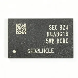
K6X0808C1D-GF55T00 - 32Kx8 SRAM 55ns 28-SOP | Samsung
MPN: K6X0808C1D-GF55T00 ✓ Active| Qty | Unit Price | Extended |
|---|---|---|
| 1 | $1.85 | $1.85 |
| 10 | $1.66 | $16.60 |
| 100 | $1.42 | $142.00 |
| 500 | $1.21 | $605.00 |
| 1,000 | $1.05 | $1,050.00 |
K6X0808C1D-GF55T00 Overview
Asynchronous SRAM is a class of random-access memory that retains data as long as power is applied, without requiring refresh clocks or address strobes. Unlike DRAM, SRAM cells are built from CMOS latches, giving the K6X0808C1D family fast, deterministic access times and a simple parallel interface of address inputs (A0-A14), eight bidirectional data lines (I/O0-I/O7), and three control pins: chip enable (CE), output enable (OE), and write enable (WE). Within the memory hierarchy it sits between register files and dense DRAM, and within power management considerations it belongs to the low-power standby class of memories.
Key features include the 55ns address access time (the GF speed grade), a wide operating voltage class supporting low data retention voltage for battery-backed applications, and CMOS technology delivering very low standby power. The device supports various operating temperature ranges and package options across the family, giving designers flexibility in industrial and consumer system design, according to the Samsung K6X0808C1D-GF55 datasheet.
Architecturally, the device decodes 15 address lines into a 32768-word memory array of 8-bit wide CMOS cells. Fully static operation means no clock, no refresh, and no timing chains, which simplifies glueless interfacing to 8-bit microcontrollers, MCUs with external memory buses, and FPGA emulated buses. Three-state outputs with OE control allow direct bus connection with other memories or peripherals.
Typical applications include battery-backed data storage in industrial control systems, code and data expansion for embedded 8/16-bit MCUs, set-top box and consumer electronics buffers, telecom line cards, and automotive electronics modules requiring non-volatile-like retention with a small backup cell.
Design consideration: for battery backup designs, drive CE high in standby to enter data retention mode; verify the retention voltage and standby current from the manufacturer datasheet for your exact temperature range.
This page synthesizes distributor availability data, same-family drop-in speed and temperature-grade alternatives, and practical design notes not found in the manufacturer datasheet.
Drop-in alternatives for K6X0808C1D-GF55T00 — same package, pin-to-pin compatible. Different-package parts requiring PCB rework are excluded.
Variants in this series
Same-series models that are drop-in compatible with K6X0808C1D-GF55T00 (same form factor and footprint) — differing in Technology, Data Bus Width, Access Time, Memory Type, Package.
Quick Comparison Tool — Select alternative parts for side-by-side comparison:
K6X0808C1D-GF55000
✅ Drop-In✓ In Stock
$3.2 / Unit
View Datasheet →K6X0808C1D-GF70000
✅ Drop-In✓ In Stock
$1.1 / Unit
View Datasheet →K6X0808C1D-BF55
✅ Drop-In✓ In Stock
$1.85 / Unit
View Datasheet →K6X0808C1D-BF70T
✅ Drop-In✓ In Stock
$1.05 / Unit
View Datasheet →K6X0808C1D-GF55T00 Maximum Ratings & Electrical Characteristics
| Memory Type | SRAM - Asynchronous |
| Memory Size | 256 Kbit |
| Organization | 32K x 8 |
| Access Time | 55 ns |
| Interface | Parallel |
| Clock Frequency | N/A (asynchronous) |
| Technology | CMOS |
| Data Retention | Low data retention voltage supported |
| Package | 28-SOP (450 mil) |
| Mounting Type | Surface Mount |
| Packaging Variant | Tape & Reel (T00 suffix) |
K6X0808C1D-GF55T00 Pin Configuration
| Pin 1 | A14 — Address input bit 14 |
| Pin 2 | A12 — Address input bit 12 |
| Pin 3 | A7 — Address input bit 7 |
| Pin 4 | A6 — Address input bit 6 |
| Pin 5 | A5 — Address input bit 5 |
| Pin 6 | A4 — Address input bit 4 |
| Pin 7 | A3 — Address input bit 3 |
| Pin 8 | A2 — Address input bit 2 |
| Pin 9 | A1 — Address input bit 1 |
| Pin 10 | A0 — Address input bit 0 |
| Pin 11 | I/O0 — Data input/output bit 0 |
| Pin 12 | I/O1 — Data input/output bit 1 |
| Pin 13 | I/O2 — Data input/output bit 2 |
| Pin 14 | GND — Ground |
| Pin 15 | I/O3 — Data input/output bit 3 |
| Pin 16 | I/O4 — Data input/output bit 4 |
| Pin 17 | I/O5 — Data input/output bit 5 |
| Pin 18 | I/O6 — Data input/output bit 6 |
| Pin 19 | I/O7 — Data input/output bit 7 |
| Pin 20 | CE — Chip enable (active low) |
| Pin 21 | A10 — Address input bit 10 |
| Pin 22 | OE — Output enable (active low) |
| Pin 23 | A11 — Address input bit 11 |
| Pin 24 | A9 — Address input bit 9 |
| Pin 25 | A8 — Address input bit 8 |
| Pin 26 | A13 — Address input bit 13 |
| Pin 27 | WE — Write enable (active low) |
| Pin 28 | VCC — Power supply |
Typical Applications
K6X0808C1D-GF55T00 is suitable for 6 applications: Battery-Backed Industrial Data Storage, External Memory Expansion for 8/16-bit MCUs, Telecom and Networking Line Cards, Consumer Electronics and Set-Top Boxes, Automotive Electronics Modules, FPGA and CPLD Emulated Memory Buses.
Battery-Backed Industrial Data Storage
In industrial controllers, metering equipment, and PLC I/O modules, the K6X0808C1D-GF55T00 stores configuration parameters, event logs, and calibration constants that must survive power loss. Its low-power CMOS design and support for low data retention voltage allow the memory to hold contents for months on a small lithium backup cell when CE is held deselected. The 55ns access time comfortably meets typical 8-bit MCU external bus timing, while the 32K x 8 organization maps directly to a single 15-bit address window. Because it is fully asynchronous and requires no refresh, the retention path is a simple diode-or supply circuit - no battery-management controller is needed.
Recommended
External Memory Expansion for 8/16-bit MCUs
Legacy and cost-sensitive microcontroller systems (8051 derivatives, H8, and similar external-bus MCUs) often lack on-chip RAM for buffers and variables. The K6X0808C1D-GF55T00 provides a glueless 32K x 8 expansion bank: 15 address lines connect to the MCU bus, I/O0-I/O7 to the data bus, and CE/OE/WE to RD/WR strobes - no external glue logic is required. The 55ns access time supports fast bus cycles that slower 70ns or 120ns SRAMs cannot meet, reducing wait states. Three-state outputs let the same bus serve flash, EEPROM, and peripherals, and the 28-SOP surface-mount package fits dense two-layer boards.
Recommended
Telecom and Networking Line Cards
Telecom line cards, protocol converters, and legacy network interface modules use fast asynchronous SRAM as frame buffers, lookup tables, and statistics counters. The K6X0808C1D-GF55T00's deterministic 55ns access - with no refresh latency - guarantees worst-case read/write timing that DRAM cannot offer, which matters for firmware that services time-slotted protocol tasks. The 32K x 8 array accommodates typical MAC address tables or HDLC buffer rings, and CMOS standby current keeps rack-level power budgets low across many populated card slots. Tape-and-reel T00 delivery suits the automated assembly of production card volumes.
Recommended
Consumer Electronics and Set-Top Boxes
Set-top boxes, DVD players, feature phones, and gaming peripherals of the classic embedded era used 32Kx8 SRAM parts like the K6X0808C1D-GF55T00 for OSD buffers, channel tables, and user settings. The device's simple asynchronous interface keeps the bill-of-materials minimal, and its wide temperature-range family options let one PCB design serve both indoor consumer and semi-outdoor variants. The 55ns speed grade supports memory-mapped graphics dot fetch loops without wait states. Because the SOP-28 footprint is shared across the whole K6X0808C1D family, cost-down moves from 55ns to 70ns grades require no layout changes.
Recommended
Automotive Electronics Modules
Body control modules, instrument clusters, and audio head units in classic automotive platforms used K6X0808C1D-family SRAM for volatile working memory and fault-code storage between ignition cycles. Selecting the correct B or G temperature grade from the family ensures operation over the required under-hood or cabin ambient range, per Samsung's family datasheet that highlights various operating temperature ranges for design flexibility. The 55ns access time supports gauge-stepping lookups and CAN message buffers on 8/16-bit MCUs, while CMOS low standby current reduces key-off battery drain when combined with a keep-alive supply feed.
Recommended
FPGA and CPLD Emulated Memory Buses
When replacing obsolete SRAM in FPGA-based retrofits, the K6X0808C1D-GF55T00 attaches directly to an FPGA bank emulating the legacy asynchronous bus. Its 55ns access time defines the worst-case FPGA read latency budget: a design meeting 55ns address-to-data timing can replicate the original board's behavior cycle-accurately. Because the device is asynchronous, no clock-domain crossing is needed - the FPGA simply drives address and control with registered outputs. The 28-SOP package hand-solders easily onto adapter boards, and low standby current suits always-on FPGA platforms where the SRAM persists configuration data.
Recommended
Recommended Products Summary
Engineering reference data for K6X0808C1D-GF55T00 — comparison, design guidance, and compliance information.
Selection Guide
Comparison with Alternatives
| Parameter | This Product | K6X0808C1D-GF55000 | K6X0808C1D-GF70000 | K6X0808C1D-BF55 | K6X0808C1D-BF70T |
|---|---|---|---|---|---|
| Package | 28-SOP (450 mil) | 28-SOP (450 mil) - same | 28-SOP (450 mil) - same | 28-SOP (450 mil) - same | 28-SOP (450 mil) - same |
| Brand | Samsung | Samsung | Samsung | Samsung | Samsung |
| Memory Organization | 32K x 8 (256 Kbit) | 32K x 8 (256 Kbit) | 32K x 8 (256 Kbit) | 32K x 8 (256 Kbit) | 32K x 8 (256 Kbit) |
| Access Time | 55 ns | 55 ns | 70 ns | 55 ns | 70 ns |
| Temperature Grade | G grade | G grade | G grade | B grade | B grade |
| Data Retention Support | Yes (low retention voltage) | Yes (same die) | Yes (same family) | Yes (same family) | Yes (same family) |
| Technology | Low-power CMOS | Low-power CMOS | Low-power CMOS | Low-power CMOS | Low-power CMOS |
Key Differentiators
- Fastest standard speed grade in the family (vs K6X0808C1D-GF70000)
- Tape-and-reel delivery for automated assembly (vs K6X0808C1D-GF55000)
- Low data retention voltage for battery backup (vs Competing 256Kbit SRAM families)
Design Notes
For battery-backed designs, hold CE high (deselected) whenever the main supply is removed - this places the SRAM in its lowest-current data retention state. Use a diode-OR (e.g., Schottky diode plus backup cell) between the main 5V rail and the retention battery, and verify the datasheet retention voltage and standby current figures for the G temperature grade at your worst-case ambient. Estimated retention duration = backup cell capacity (Ah) divided by standby current (A); always derate by 50% for cell aging.
Place a 0.1uF ceramic decoupling capacitor within 3 mm of the VCC pin (pin 28) with a solid via to the ground plane near GND (pin 14). Although asynchronous SRAM generates little switching noise itself, the data bus it drives can; a short ground return path under the SOP-28 keeps I/O ground bounce below the VOH/VOL margins during fast 55ns bus cycles. Avoid routing address lines under the package to reduce coupling into the memory array sense paths.
Never assert CE and WE low simultaneously during power-up or power-down - a write cycle with an unstable VCC can corrupt the addressed cell. Add a power-supply supervisor (such as a reset IC with active-low MR) that gates WE until the bus MCU is out of reset. Also confirm the speed grade in your timing closure: a 70ns alternative is pin-compatible but will fail 55ns bus timing, so lock the GF55 MPN in the BOM if your address-to-data window is under 70ns.
Compliance Information
Compliance status not stated in the retrieved distributor listings; verify against the Samsung product page or ask the distributor for a material declaration before export-controlled or EU shipments.