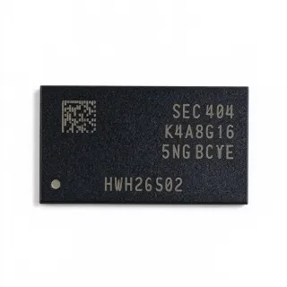
K6X0808C1D-GF70T00 - 256Kbit 32Kx8 Async SRAM 70ns | Samsung
MPN: K6X0808C1D-GF70T00 ✓ Active| Qty | Unit Price | Extended |
|---|---|---|
| 1 | $3.2 | $3.20 |
| 10 | $2.85 | $28.50 |
| 100 | $2.45 | $245.00 |
| 500 | $2.1 | $1,050.00 |
| 1,000 | $1.85 | $1,850.00 |
K6X0808C1D-GF70T00 Overview
Static RAM (SRAM) is a type of volatile semiconductor memory that stores each bit in a bistable latch circuit, so data is retained as long as power is applied and no refresh cycles are required, unlike DRAM. Within the memory IC hierarchy, SRAM sits alongside DRAM, EEPROM and Flash as a solid-state memory family, and asynchronous SRAM specifically means accesses are controlled purely by address, chip-enable (CE), output-enable (OE) and write-enable (WE) pins with no external clock.
Key features include the fast 70 ns address access time, a fully static design requiring no clock or refresh, CMOS technology for low power consumption, and TTL-compatible I/O levels that simplify interfacing with legacy 5 V microcontrollers and microprocessors. The three control lines (CE, OE, WE) allow easy bus-mastering, bank selection and read/write gating in 8-bit systems.
Fabricated on Samsung's advanced CMOS process, the K6X0808C1D family supports various operating temperature ranges and multiple package types for system design flexibility, according to the manufacturer datasheet. The simple asynchronous interface keeps timing design straightforward: address setup, CE/OE access, and write pulse widths all fall within the 70 ns speed grade budget.
Typical applications include 5 V embedded controllers, industrial equipment retrofits and spare-part repairs, telecom line cards, test and measurement instruments, and buffer memory in legacy 8-bit and 16-bit microprocessor systems that use JEDEC-standard 32K x 8 SRAM footprints.
A key design consideration is power integrity: decouple the 5 V rail with a 0.1 uF ceramic capacitor close to pin 28, and ensure CE is actively driven because deselected standby current is far lower than active current. Avoid floating the control lines during power-up to prevent spurious writes.
This page adds unique value beyond the datasheet by consolidating drop-in alternatives, distributor pricing context, pinout, and practical design notes for sourcing and repair engineers.
Drop-in alternatives for K6X0808C1D-GF70T00 — same package, pin-to-pin compatible. Different-package parts requiring PCB rework are excluded.
Variants in this series
Same-series models that are drop-in compatible with K6X0808C1D-GF70T00 (same form factor and footprint) — differing in Memory Type, Package, Data Bus Width, Access Time, Organization.
Quick Comparison Tool — Select alternative parts for side-by-side comparison:
K6X0808C1D-GF70000
✅ Drop-In✓ In Stock
$1.1 / Unit
View Datasheet →K6X0808C1D-GF55T00
✅ Drop-In✓ In Stock
$1.05 / Unit
View Datasheet →K6X0808C1D-BF70T
✅ Drop-In✓ In Stock
$1.05 / Unit
View Datasheet →K6X0808C1D-BF55
✅ Drop-In✓ In Stock
$1.85 / Unit
View Datasheet →IS62C256AL-70
✅ Drop-In📋 Reference alternative (not in catalog)
AS6C256-70SIN
✅ Drop-In📋 Reference alternative (not in catalog)
K6X0808C1D-GF70T00 Specifications
| Memory Type | SRAM - Asynchronous |
| Memory Size | 256 Kbit |
| Organization | 32K x 8 |
| Access Time | 70 ns |
| Interface | Parallel |
| Technology | CMOS |
| Supply Voltage | 5 V |
| Mounting Type | Surface Mount |
| Package | 28-SOP |
| I/O Type | Common Data I/O, TTL compatible |
| Control Signals | CE, OE, WE |
| Clock / Refresh | Fully static, no clock or refresh required |
| Packaging | Tape & Reel (T00 suffix) |
K6X0808C1D-GF70T00 Pin Configuration
| Pin 1 | A14 — Address input bit 14 |
| Pin 2 | A12 — Address input bit 12 |
| Pin 3 | A7 — Address input bit 7 |
| Pin 4 | A6 — Address input bit 6 |
| Pin 5 | A5 — Address input bit 5 |
| Pin 6 | A4 — Address input bit 4 |
| Pin 7 | A3 — Address input bit 3 |
| Pin 8 | A2 — Address input bit 2 |
| Pin 9 | A1 — Address input bit 1 |
| Pin 10 | A0 — Address input bit 0 |
| Pin 11 | I/O0 — Data input/output bit 0 |
| Pin 12 | I/O1 — Data input/output bit 1 |
| Pin 13 | I/O2 — Data input/output bit 2 |
| Pin 14 | GND — Ground |
| Pin 15 | I/O3 — Data input/output bit 3 |
| Pin 16 | I/O4 — Data input/output bit 4 |
| Pin 17 | I/O5 — Data input/output bit 5 |
| Pin 18 | I/O6 — Data input/output bit 6 |
| Pin 19 | I/O7 — Data input/output bit 7 |
| Pin 20 | CE — Chip enable (active low) |
| Pin 21 | A10 — Address input bit 10 |
| Pin 22 | OE — Output enable (active low) |
| Pin 23 | A11 — Address input bit 11 |
| Pin 24 | A9 — Address input bit 9 |
| Pin 25 | A8 — Address input bit 8 |
| Pin 26 | A13 — Address input bit 13 |
| Pin 27 | WE — Write enable (active low) |
| Pin 28 | VCC — Power supply, 5 V |
Typical Applications
K6X0808C1D-GF70T00 is suitable for 6 applications: Legacy 5V Embedded Controllers, Industrial Equipment Repair and Sustaining Engineering, Telecom Line Cards and Network Equipment, Test and Measurement Instruments, Battery-Backed Data Retention Modules, Retrofit and Upgrade of 8-bit Microprocessor Boards.
Legacy 5V Embedded Controllers
The K6X0808C1D-GF70T00 fits legacy 5 V microcontroller and microprocessor systems that use the JEDEC 62256-class 32K x 8 SRAM footprint. Its 70 ns access time comfortably supports 8 MHz-class bus timings, and TTL-compatible common I/O lines connect directly to processors such as the 8051, 68HC11, Z80 and early 16-bit MPUs without level shifting. Because the device is fully static, no refresh controller or bus arbitration logic is needed, preserving the original board design. The 28-SOP surface-mount package allows direct reflow onto existing land patterns during board repair or re-manufacture of legacy industrial and telecom controllers.
Recommended
Industrial Equipment Repair and Sustaining Engineering
PLCs, motor drives, process controllers and CNC equipment from the 1990s and 2000s frequently used 5 V, 32K x 8 asynchronous SRAM such as the K6X0808C1D-GF70T00 for parameter and data storage. When these devices fail, the Samsung part restores form-fit-function without PCB modification. Its fully static CMOS design means the replacement simply drops into the 28-SOP socket or land pattern, and the 70 ns timing matches the original bus budget. Distributors including DigiKey Marketplace and Precision Logic stock the part specifically for repair quantities, making it a sustaining-engineering staple for factory maintenance teams extending machine life.
Recommended
Telecom Line Cards and Network Equipment
Telecom line cards, channel banks and legacy transmission equipment commonly used 32K x 8 SRAM as frame buffers, lookup tables and configuration memory. The K6X0808C1D-GF70T00's 70 ns access time supports channel-sampled data buffering, while its low CMOS standby current keeps power budgets within card limits when memory banks are deselected via CE. The three-line control interface (CE, OE, WE) allows simple bank selection in multi-chip memory arrays typical of line-card designs. The 28-SOP package withstands standard reflow profiles, supporting card-level rework in network maintenance depots still servicing legacy T1/E1 and PBX hardware.
Recommended
Test and Measurement Instruments
Oscilloscopes, data loggers, bench power supplies and signal generators of the 5 V generation used asynchronous SRAM for waveform capture buffers and calibration storage. The K6X0808C1D-GF70T00's deterministic 70 ns access time provides consistent read latency across the full operating range, which matters for calibrated timing paths in instruments. Its 32K x 8 organization offers 32 KB of buffer capacity per device, and multiple devices can be CE-decoded in parallel to expand capture depth. Fully static operation eliminates refresh noise that could couple into sensitive analog front ends, preserving measurement integrity in mixed-signal instrument boards.
Recommended
Battery-Backed Data Retention Modules
In battery-backed memory modules and NVRAM-style assemblies, low standby current is the deciding parameter, and the CMOS K6X0808C1D-GF70T00 addresses this by drawing minimal current when CE is deselected. A backup cell or supercapacitor on the 5 V rail retains SRAM contents through main-power loss, preserving configuration and log data in meters, access controllers and medical equipment. The fully static design tolerates the slowly decaying supply of a discharging battery without corruption, provided CE is actively held high. Designers should verify the datasheet standby specification and size the backup source for the required retention interval.
Recommended
Retrofit and Upgrade of 8-bit Microprocessor Boards
Retrofitting EPROM-based or DRAM-based memory subsystems with reliable static RAM is a common upgrade path for vintage computers, arcade boards and industrial 8-bit systems. The K6X0808C1D-GF70T00 replaces the classic 62256 SRAM and 28-pin EPROM footprints (with minor WE-line wiring) to eliminate refresh circuitry and improve reliability. Its 70 ns access time meets or exceeds the 150-450 ns timing of the parts it typically replaces, adding timing margin. The 28-SOP package suits both new adapter PCBs and direct surface-mount replacement, and battery-backed circuits can be added for non-volatile behavior.
Recommended
Recommended Products Summary
Engineering reference data for K6X0808C1D-GF70T00 — comparison, design guidance, and compliance information.
Selection Guide
Comparison with Alternatives
| Parameter | This Product | K6X0808C1D-GF70000 | K6X0808C1D-GF55T00 | K6X0808C1D-BF70T | IS62C256AL-70 | AS6C256-70SIN |
|---|---|---|---|---|---|---|
| Package | 28-SOP | 28-SOP - same | 28-SOP - same | 28-SOP - same | 28-SOP - same footprint | 28-SOP - same footprint |
| Brand | Samsung | Samsung | Samsung | Samsung | ISSI | Alliance Memory |
| Organization | 32K x 8 | 32K x 8 | 32K x 8 | 32K x 8 | 32K x 8 | 32K x 8 |
| Access Time | 70 ns | 70 ns | 55 ns | 70 ns | 70 ns | 70 ns |
| Memory Size | 256 Kbit | 256 Kbit | 256 Kbit | 256 Kbit | 256 Kbit | 256 Kbit |
| Supply Voltage | 5 V | 5 V | 5 V | 5 V | 5 V | 5 V |
Key Differentiators
- Exact legacy form-fit-function (vs IS62C256AL-70)
- Faster timing headroom available in-family (vs K6X0808C1D-BF70T)
- Supply security via same-footprint cross-brand options (vs AS6C256-70SIN)
Design Notes
Decouple the 5 V supply with a 0.1 uF ceramic capacitor placed within 5 mm of pin 28 (VCC) and pin 14 (GND); add a 4.7-10 uF bulk capacitor per memory bank on multi-chip boards. Keep address and data traces under 10 cm where possible, and avoid routing WE near clock lines to prevent glitch-coupled writes. For socketed repair work, clean SOP pads thoroughly and verify pin 1 orientation against the dot marker before reflow.
Never allow CE, WE or OE to float during power-up, power-down or processor reset. A floating write-enable can generate spurious write cycles that corrupt memory contents - the most common field failure attributed to 'bad SRAM'. Add a pull-up resistor (typically 10 kohm) on CE and WE so the device stays deselected during bus transitions, and gate WE with the system reset signal in battery-backed designs.
CMOS SRAM active current scales with access rate; standby current is reached only when CE is high. In low-power or battery-backed designs, decode CE so the device is deselected whenever the bus is idle, and avoid resistive pull-downs on data lines that fight the tri-stated outputs. Verify actual standby and active current figures in the Samsung family datasheet before sizing backup cells for retention-critical applications.
Compliance Information
Compliance data was not stated in the verified web data retrieved for this legacy part; request RoHS/REACH certificates from the distributor or Samsung before production use.