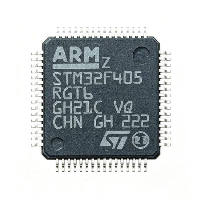
STM32F405RGT6 - MCU Cortex-M4F de 168MHz, 1MB de Flash | STMicroelectronics
N.º de pieza: STM32F405RGT6 ✓ Activo| Cant. | Precio unitario | Total |
|---|---|---|
| 1 | $11.5 | $11,50 |
| 10 | $10.2 | $102,00 |
| 100 | $8.85 | $885,00 |
| 500 | $7.6 | $3.800,00 |
| 1.000 | $6.75 | $6.750,00 |
STM32F405RGT6 Descripción general
Un microcontrolador (MCU) es un circuito integrado compacto que combina un núcleo de procesador, memoria volátil y no volátil, y periféricos programables en un único dado de silicio para gobernar operaciones específicas en sistemas embebidos. El STM32F405RGT6 pertenece a la línea de rendimiento convencional STM32F4, que se sitúa dentro de la amplia familia STM32 de microcontroladores Flash de 32 bits. La jerarquía de categorías es MCU -> MCU de 32 bits -> MCU ARM Cortex-M -> MCU Cortex-M4 -> MCU STM32F4. Los MCU son el elemento de control central en la electrónica industrial, de consumo, médica e IoT.
Las características clave incluyen 3 ADC de 12 bits (2,4 MSPS), 2 DAC de 12 bits, 12 temporizadores de 16 bits más 2 temporizadores de 32 bits, 51 GPIO y una conectividad completa: 3 I2C, 4 USART más 2 UART, 3 SPI, 2 CAN, USB 2.0 OTG Full-Speed y High-Speed con PHY integrado, Ethernet de 100 Mbit, SDIO y una interfaz de cámara DCMI. El dispositivo funciona de 1,8 V a 3,6 V e incluye un generador de números aleatorios verdadero, una unidad CRC por hardware y un ID de dispositivo único de 96 bits.
Técnicamente, el chip utiliza un proceso CMOS de 90 nm con un ART Accelerator que permite la ejecución sin estados de espera desde la Flash, maximizando el rendimiento efectivo del Cortex-M4. Una unidad de protección de memoria admite un aislamiento de firmware robusto, mientras que múltiples modos de bajo consumo (Sleep, Stop, Standby con RTC) permiten optimizar la energía en diseños alimentados por batería. El PHY USB OTG HS integrado y la MAC Ethernet eliminan el costo de BOM de PHY externos en muchos diseños.
Las aplicaciones típicas incluyen accionamientos de motor con control orientado al campo (servoaccionamientos FOC que aprovechan la FPU y las instrucciones DSP), conversión de potencia digital y etapas PFC, controladores PLC y de automatización industrial, periféricos USB y dispositivos de audio, y productos de consumo/médicos que requieren procesamiento de señales en tiempo real. El ecosistema de código abierto STM32CubeIDE y STM32CubeMX con bibliotecas HAL/LL acorta significativamente los ciclos de desarrollo.
Consideración de diseño: proporcione un desacoplamiento adecuado de 100 nF en cada par de pines VDD/VSS, enrute USB HS D+/D- como un par diferencial de 90 ohmios y mantenga las pistas SDIO con longitudes igualadas. Tenga en cuenta también que los estados de espera de Flash se aplican por encima de 168 MHz si se modifica la configuración del ART Accelerator.
Esta página sintetiza precios de distribuidores, alternativas drop-in verificadas y notas de diseño prácticas no consolidadas en la hoja de datos del fabricante.
Alternativas directas para STM32F405RGT6 — mismo encapsulado, compatible pin a pin. Se excluyen las piezas de otro encapsulado que requieren retrabajo de la PCB.
Variantes de esta serie
Modelos de la misma serie compatibles directamente con STM32F405RGT6 (mismo factor de forma y huella) — difiere en SRAM, Package, ADC, Timers, Flash Memory.
Herramienta de comparación rápida — seleccione piezas alternativas para compararlas lado a lado:
STM32F415RGT6
✓ En stock
$8.1 / unidad
Ver hoja de datos →STM32F405ZGT6
✓ En stock
$8.1 / unidad
Ver hoja de datos →STM32F405VGT6
✓ En stock
$8.1 / unidad
Ver hoja de datos →STM32F407VGT6
✓ En stock
$7.55 / unidad
Ver hoja de datos →STM32F405RGT7
✓ En stock
$7.95 / unidad
Ver hoja de datos →GD32F405RGT6
📋 Alternativa de referencia (no en el catálogo)
STM32F405RGT6 Valores máximos y características eléctricas
| Core | ARM Cortex-M4F (with single-precision FPU and DSP) |
| Frecuencia de reloj máxima | 168 MHz |
| Performance | 210 DMIPS (1.25 DMIPS/MHz) |
| Flash Memory | 1 MB (1M x 8) |
| SRAM | 192 KB (including 4 KB backup SRAM) |
| Operating Voltage | 1.8 V to 3.6 V |
| Encapsulado | 64-LQFP (10x10 mm) |
| GPIO Count | 51 |
| ADC | 3x 12-bit, 2.4 MSPS, up to 24 channels |
| DAC | 2x 12-bit |
| Timers | 12x 16-bit + 2x 32-bit |
| Communication Interfaces | 3x I2C, 4x USART + 2x UART, 3x SPI, 2x CAN, USB OTG FS/HS, 100M Ethernet, SDIO, DCMI |
| Rango de temperatura de funcionamiento | -40C to +85C |
| Tipo de montaje | Surface Mount |
| Estado RoHS | Compliant |
| Lead-Free / Halogen-Free | Yes |
Configuración de pines de STM32F405RGT6
| Pin 1 | VBAT — Battery domain supply for RTC and backup SRAM |
| Pin 2 | PC13 — GPIO/Tamper-RTC (standard I/O with interrupt) |
| Pin 3 | PC14 — GPIO/OSC32_IN (32.768 kHz crystal) |
| Pin 4 | PC15 — GPIO/OSC32_OUT (32.768 kHz crystal) |
| Pin 5 | OSC_IN — HSE crystal/clock input |
| Pin 6 | OSC_OUT — HSE crystal output |
| Pin 7 | NRST — Reset input (active low) |
| Pin 8 | VSSA — Analog ground |
| Pin 9 | VDDA — Analog supply (1.8-3.6V) |
| Pin 10 | PA0-WKUP — GPIO/ADC0_IN0/Wakeup |
| Pin 11 | PA1 — GPIO/ADC0_IN1 |
| Pin 12 | PA2 — GPIO/USART2_TX/ADC0_IN2 |
| Pin 13 | PA3 — GPIO/USART2_RX/ADC0_IN3 |
| Pin 14 | PA4 — GPIO/SPI1_NSS/DAC_OUT1 |
| Pin 15 | PA5 — GPIO/SPI1_SCK/DAC_OUT2 |
| Pin 16 | PA6 — GPIO/SPI1_MISO/ADC1_IN2 |
| Pin 17 | PA7 — GPIO/SPI1_MOSI/ADC1_IN3 |
| Pin 18 | PB0 — GPIO/ADC2_IN8/TIM3_CH3 |
| Pin 19 | PB1 — GPIO/ADC2_IN9/TIM3_CH4 |
| Pin 20 | VSS_1 — Digital ground |
| Pin 21 | VDD_1 — Digital supply (1.8-3.6V) |
| Pin 22 | PB2/BOOT1 — GPIO/BOOT1 input |
| Pin 23 | PB10 — GPIO/I2C2_SCL/USART3_TX |
| Pin 24 | PB11 — GPIO/I2C2_SDA/USART3_RX |
| Pin 25 | VSS_2 — Digital ground |
| Pin 26 | VDD_2 — Digital supply (1.8-3.6V) |
| Pin 27 | PB12 — GPIO/SPI2_NSS/CAN2_RX |
| Pin 28 | PB13 — GPIO/SPI2_SCK/CAN2_TX |
| Pin 29 | PB14 — GPIO/SPI2_MISO/TIM12_CH1 |
| Pin 30 | PB15 — GPIO/SPI2_MOSI/TIM12_CH2 |
| Pin 31 | PA8 — GPIO/TIM1_CH1/USART1_CK/MCO |
| Pin 32 | PA9 — GPIO/USART1_TX/TIM1_CH2 |
| Pin 33 | PA10 — GPIO/USART1_RX/TIM1_CH3 |
| Pin 34 | PA11 — GPIO/USB_DM/CAN1_RX/TIM1_CH4 |
| Pin 35 | PA12 — GPIO/USB_DP/CAN1_TX/TIM1_ETR |
| Pin 36 | PA13 — GPIO/SWDIO |
| Pin 37 | VSS_3 — Digital ground |
| Pin 38 | VDD_3 — Digital supply (1.8-3.6V) |
| Pin 39 | PA14 — GPIO/SWCLK |
| Pin 40 | PA15 — GPIO/SPI3_NSS/TIM2_CH1 |
| Pin 41 | PC6 — GPIO/USART6_TX/TIM3_CH1 |
| Pin 42 | PC7 — GPIO/USART6_RX/TIM3_CH2 |
| Pin 43 | PC8 — GPIO/SDIO_D0/TIM3_CH3 |
| Pin 44 | PC9 — GPIO/SDIO_D1/TIM3_CH4 |
| Pin 45 | PA0 — GPIO/WKUP/USART2_CTS |
| Pin 46 | VDD_4 — Digital supply (1.8-3.6V) |
| Pin 47 | VSS_4 — Digital ground |
| Pin 48 | PB3 — GPIO/SPI3_SCK/TIM2_CH2 |
| Pin 49 | PB4 — GPIO/SPI3_MISO/TIM3_CH1 |
| Pin 50 | PB5 — GPIO/SPI3_MOSI/I2C1_SMBA |
| Pin 51 | PB6 — GPIO/I2C1_SCL/TIM4_CH1/USART1_TX |
| Pin 52 | PB7 — GPIO/I2C1_SDA/TIM4_CH2/USART1_RX |
| Pin 53 | BOOT0 — Boot mode select |
| Pin 54 | PB8 — GPIO/I2C1_SCL/CAN1_RX/TIM4_CH3 |
| Pin 55 | PB9 — GPIO/I2C1_SDA/CAN1_TX/TIM4_CH4 |
| Pin 56 | VSS_5 — Digital ground |
| Pin 57 | VDD_5 — Digital supply (1.8-3.6V) |
| Pin 58 | PD0 — GPIO/FSMC_D2/CAN1_RX |
| Pin 59 | PD1 — GPIO/FSMC_D3/CAN1_TX |
| Pin 60 | VREF+ — ADC positive reference |
| Pin 61 | VSSA — Analog ground |
| Pin 62 | VDDA — Analog supply |
| Pin 63 | PA13 — GPIO (secondary) |
| Pin 64 | VSS — Ground (additional) |
Aplicaciones típicas
STM32F405RGT6 es adecuado para 7 aplicacións: Field-Oriented-Control Motor Drives, Industrial USB Host Peripherals, Digital Power Conversion and PFC, Audio Processing and DAC/ADC Interfaces, Industrial Ethernet Gateways, Consumer Medical Devices, Drones and Robotics Controllers.
Field-Oriented-Control Motor Drives
The STM32F405RGT6 fits FOC motor drives because the Cortex-M4F FPU and DSP instructions accelerate Park/Clarke transforms and PID loops by roughly 2-3x versus a Cortex-M3. The 168 MHz clock headroom leaves 30-40 percent CPU margin for encoder decoding and current-loop control. The 3x 12-bit ADCs sample phase currents at 2.4 MSPS, while the 12 timers provide complementary PWM with hardware dead-time insertion. Place a 100 nF decoupling cap on every VDD pin and route ADC inputs away from PWM switching nodes to preserve SNR.
Recomendado
Industrial USB Host Peripherals
The STM32F405RGT6 is widely used in industrial USB host peripherals because the integrated USB OTG Full-Speed and High-Speed PHY eliminates an external ULPI chip, reducing BOM by approximately USD 1-2. The Cortex-M4F core handles USB stack processing and application logic simultaneously. The SDIO controller and FSMC bus (on the F407 family variant) support external data buffering for printers, scanners, and data loggers. Designers should route the 90-ohm USB differential pair with length matching within 150 mil and add ESD protection diodes.
Recomendado
Digital Power Conversion and PFC
The STM32F405RGT6 is well-suited to digital power conversion and PFC stages because the Cortex-M4F single-precision FPU accelerates multiply-accumulate loops used in PID, state-space, and predictive control algorithms. The 12-bit ADCs sampled at 2.4 MSPS capture current and voltage waveforms with adequate bandwidth for PFC at 50-100 kHz switching. The high-resolution timer (217 ps) generates phase-shifted PWM for bridgeless PFC topologies. Plan 4-layer PCB layout to keep switching noise away from analog signal paths.
Recomendado
Audio Processing and DAC/ADC Interfaces
The STM32F405RGT6 serves audio processing applications because the Cortex-M4F SIMD instructions accelerate FFT, biquad, and dynamics processing at 48 kHz sample rates. The 2x 12-bit DACs and 3x 12-bit ADCs integrate codec functionality for budget audio products. The I2S-capable SPI port supports external 24-bit codecs. The 192 KB SRAM buffers multiple audio frames without external memory. Use DMA for both I2S RX and TX to keep the core free for DSP processing.
Recomendado
Industrial Ethernet Gateways
The STM32F405RGT6 fits industrial Ethernet gateways because the integrated 100 Mbit/s MAC and RMII interface connect to any standard Ethernet PHY for Modbus TCP, EtherNet/IP, or PROFINET. The Cortex-M4F core runs TCP/IP stacks plus application logic without external memory. The CAN 2.0B peripherals bridge fieldbus to enterprise networks. Pair with a wide-input DC-DC and provide 2 kV galvanic isolation on the Ethernet magnetics for industrial EMC compliance.
Recomendado
Consumer Medical Devices
The STM32F405RGT6 powers consumer medical devices like blood-pressure monitors, pulse oximeters, and spirometers because the Cortex-M4F core runs sensor-fusion DSP while the 12-bit ADC captures analog biosignals with 2.4 MSPS. The 1 MB Flash accommodates FDA-21CFR-Part-11 firmware with bootloader and OTA update. The USB OTG port provides powered device charging and data sync. Use the RTC with battery domain to maintain accurate timestamps across power cycles.
Recomendado
Drones and Robotics Controllers
The STM32F405RGT6 is a popular flight-controller MCU in hobbyist and commercial drones because the Cortex-M4F core runs Betaflight/Cleanflight/INAV firmware with full PID loops at 8 kHz update rates. The 168 MHz clock plus FPU computes quaternion math at rates that 72 MHz Cortex-M3 parts struggle to maintain. The 3x SPI ports connect to gyros, barometers, and radio receivers simultaneously. Mount the LQFP-64 with thermal vias to a copper pour for thermal relief at 50-60 mA active current.
Recomendado
Resumen de productos recomendados
Datos de referencia de ingeniería para STM32F405RGT6 — comparación, orientación de diseño e información de cumplimiento.
Guía de selección
Comparación con alternativas
| Parámetro | Este producto | STM32F415RGT6 | STM32F405RGT7 | STM32F405ZGT6 | GD32F405RGT6 |
|---|---|---|---|---|---|
| Brand | STMicroelectronics | STMicroelectronics | STMicroelectronics | STMicroelectronics | GigaDevice |
| Package | 64-LQFP (10x10 mm) | 64-LQFP (10x10 mm) - same | 64-LQFP (10x10 mm) - same | 144-LQFP (20x20 mm) | 64-LQFP (10x10 mm) - same |
| Core | Cortex-M4F @ 168 MHz | Cortex-M4F @ 168 MHz | Cortex-M4F @ 168 MHz | Cortex-M4F @ 168 MHz | Cortex-M4F @ 168 MHz |
| Flash | 1 MB | 1 MB | 1 MB | 1 MB | 1 MB |
| SRAM | 192 KB | 192 KB | 192 KB | 192 KB | 192 KB |
| Crypto/Hash Engine | No | Yes (AES, SHA) | No | No | No |
| Operating Temperature | -40C to +85C | -40C to +85C | -40C to +105C | -40C to +85C | -40C to +85C |
| GPIO Count | 51 | 51 | 51 | 114 | 51 |
| Approx. Unit Price (1k qty) | USD 6.75 | USD 7.40 | USD 6.95 | USD 9.10 | USD 3.20 (GigaDevice, LCSC) |
Diferenciadores clave
- PHY USB OTG High-Speed integrado (frente a STM32F103RCT6 (Cortex-M3))
- FPU de precisión simple con instrucciones DSP (frente a STM32F103C8T6 (Cortex-M3))
- 1 MB de Flash frente a la base típica de 256-512 KB de Cortex-M3 (frente a GD32F103RCT6)
Notas de diseño
Proporcione un condensador de desacoplamiento de 100 nF en cada par de pines VDD/VSS, colocado a menos de 2 mm del pin. Añada un cerámico de 4,7 uF de bulk cerca del grupo VDD-1/VSS-1 y un tantalio o cerámico de 10 uF en la salida del regulador. Para el funcionamiento de USB OTG HS, el PHY interno requiere que la alimentación VDD-USB esté estable dentro del 90 por ciento del valor nominal antes de habilitar el PLL; de lo contrario, la enumeración fallará. Estimado: suponiendo una corriente activa de 100 mA a 3,3 V, la potencia total es de 330 mW; el theta_JA del LQFP-64 de aproximadamente 50 C/W produce un aumento de 16C sobre la temperatura ambiente, muy dentro de los límites seguros.
Enrute el par USB OTG HS D+/D- como un par diferencial de 90 ohmios con longitudes igualadas dentro de 150 mil y sin stubs. Mantenga las pistas del cristal cortas (menos de 5 mm) y protéjalas con un plano de masa. Las señales RMII de Ethernet deben tener longitudes igualadas dentro de 50 mil respecto al PHY externo. Las pistas SDIO deben tener longitudes igualadas dentro de 100 mil y enrutarse en la capa interna con un plano de referencia ininterrumpido. Utilice un stackup de 4 capas con un plano GND continuo debajo del MCU para la integridad del camino de retorno.
No habilite el PLL por encima de 168 MHz sin confirmar la configuración de estados de espera de Flash; cero estados de espera solo es válido hasta 168 MHz. BOOT0 debe conectarse a bajo para el arranque normal desde Flash o dejarse flotante si no se usa; dejarlo alto lleva al MCU al bootloader de memoria del sistema. Para la precisión del ADC, asegúrese de que VDDA esté desacoplada con una combinación de 100 nF + 1 uF y que VREF+ tenga un condensador de 100 nF a VSSA. El pad expuesto central del LQFP-64 (si está presente) debe soldarse a un pad de masa para la disipación térmica.
Coloque el cristal HSE a menos de 5 mm de los pines OSC_IN/OSC_OUT con pistas cortas y simétricas. Enrute las señales de depuración SWD/SWCLK lejos de nodos de conmutación de alta corriente. Coloque las resistencias pull-up de modo de arranque y reset junto al MCU. Proporcione un pad TEST en PA13/PA14 para programación de fábrica. La línea NRST necesita un condensador de 100 nF más una resistencia pull-up de 10 kohm a VDD y debe exponerse en un conector para la capacidad de reset en el sistema.
Información de cumplimiento
RoHS compliant per ST product page. Not AEC-Q100 qualified; for automotive designs use the STM32F405RGT6-V variant or a different family member.


