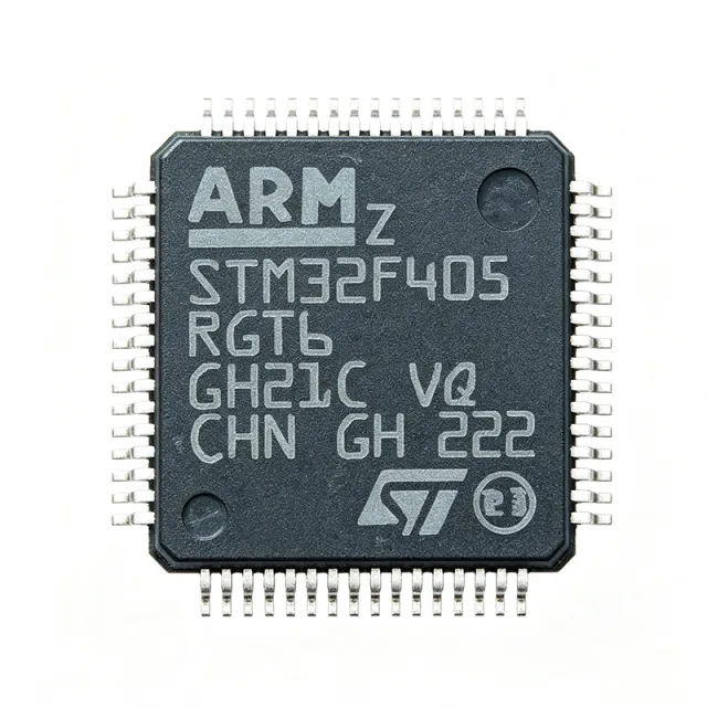
STM32F405RGT6 - 168MHz Cortex-M4F,1MB Flash MCU | STMicroelectronics
料号: STM32F405RGT6 ✓ 量产中| 数量 | 单价 | 小计 |
|---|---|---|
| 1 | $11.5 | $11.50 |
| 10 | $10.2 | $102.00 |
| 100 | $8.85 | $885.00 |
| 500 | $7.6 | $3,800.00 |
| 1,000 | $6.75 | $6,750.00 |
STM32F405RGT6 概述
微控制器(MCU)是一种紧凑的集成电路,将处理器内核、易失性和非易失性存储器以及可编程外设集成在单个硅片上,用于控制嵌入式系统中的特定操作。STM32F405RGT6 属于 STM32F4 主流性能系列,该系列隶属于更广泛的 STM32 32 位 Flash 微控制器家族。类别层级为 MCU -> 32 位 MCU -> ARM Cortex-M MCU -> Cortex-M4 MCU -> STM32F4 MCU。MCU 是工业、消费、医疗和物联网电子设备中的核心控制元件。
主要特性包括 3 个 12 位 ADC(2.4 MSPS)、2 个 12 位 DAC、12 个 16 位定时器加 2 个 32 位定时器、51 个 GPIO,以及丰富的连接性:3 个 I2C、4 个 USART 加 2 个 UART、3 个 SPI、2 个 CAN、带片上 PHY 的 USB 2.0 OTG 全速和高速、100Mbit 以太网、SDIO 和 DCMI 摄像头接口。该器件工作电压为 1.8V 至 3.6V,并包含真随机数发生器、硬件 CRC 单元和 96 位唯一器件 ID。
技术上,该芯片采用 90 nm CMOS 工艺,配备 ART 加速器,可实现从 Flash 零等待状态执行,最大化有效 Cortex-M4 吞吐量。存储器保护单元支持稳健的固件隔离,而多种低功耗模式(睡眠、停止、带 RTC 的待机)可为电池供电设计优化能耗。集成的 USB OTG HS PHY 和以太网 MAC 为许多设计消除了外部 PHY 的 BOM 成本。
典型应用包括磁场定向控制电机驱动(利用 FPU 和 DSP 指令的 FOC 伺服驱动)、数字电源转换和 PFC 级、工业 PLC 和自动化控制器、USB 外设和音频设备,以及需要实时信号处理的消费/医疗产品。开源 STM32CubeIDE 和 STM32CubeMX 生态系统及 HAL/LL 库可显著缩短开发周期。
设计注意事项:在每个 VDD/VSS 引脚对提供足够的 100 nF 去耦,将 USB HS D+/D- 作为 90 欧姆差分对布线,并保持 SDIO 走线长度匹配。另请注意,如果更改 ART 加速器配置,在 168 MHz 以上将适用 Flash 等待状态。
本页面综合了分销商定价、经验证的直接替代品以及制造商数据手册中未整合的实用设计说明。
直接替换替代料: STM32F405RGT6 ——相同封装,引脚兼容。需要 PCB 改动的不同封装料号已排除。
本系列中的变体
可与以下型号直接替换的同系列型号: STM32F405RGT6 (相同外形与封装尺寸) ——差异在于 SRAM, ADC, Package, Timers, Flash Memory.
快速对比工具——选择替代料号进行并排对比:
STM32F415RGT6
✓ 有现货
$8.1 / 个
查看数据手册 →STM32F405ZGT6
✓ 有现货
$8.1 / 个
查看数据手册 →STM32F405VGT6
✓ 有现货
$8.1 / 个
查看数据手册 →STM32F407VGT6
✓ 有现货
$7.55 / 个
查看数据手册 →STM32F405RGT7
📋 参考替代料(不在目录中)
GD32F405RGT6
📋 参考替代料(不在目录中)
STM32F405RGT6 最大额定值与电气特性
| Core | ARM Cortex-M4F (with single-precision FPU and DSP) |
| 最大时钟频率 | 168 MHz |
| Performance | 210 DMIPS (1.25 DMIPS/MHz) |
| Flash Memory | 1 MB (1M x 8) |
| SRAM | 192 KB (including 4 KB backup SRAM) |
| Operating Voltage | 1.8 V to 3.6 V |
| 封装 | 64-LQFP (10x10 mm) |
| GPIO Count | 51 |
| ADC | 3x 12-bit, 2.4 MSPS, up to 24 channels |
| DAC | 2x 12-bit |
| Timers | 12x 16-bit + 2x 32-bit |
| Communication Interfaces | 3x I2C, 4x USART + 2x UART, 3x SPI, 2x CAN, USB OTG FS/HS, 100M Ethernet, SDIO, DCMI |
| 工作温度范围 | -40C to +85C |
| 安装类型 | Surface Mount |
| RoHS 状态 | Compliant |
| Lead-Free / Halogen-Free | Yes |
STM32F405RGT6 引脚配置
| 引脚 1 | VBAT — Battery domain supply for RTC and backup SRAM |
| 引脚 2 | PC13 — GPIO/Tamper-RTC (standard I/O with interrupt) |
| 引脚 3 | PC14 — GPIO/OSC32_IN (32.768 kHz crystal) |
| 引脚 4 | PC15 — GPIO/OSC32_OUT (32.768 kHz crystal) |
| 引脚 5 | OSC_IN — HSE crystal/clock input |
| 引脚 6 | OSC_OUT — HSE crystal output |
| 引脚 7 | NRST — Reset input (active low) |
| 引脚 8 | VSSA — Analog ground |
| 引脚 9 | VDDA — Analog supply (1.8-3.6V) |
| 引脚 10 | PA0-WKUP — GPIO/ADC0_IN0/Wakeup |
| 引脚 11 | PA1 — GPIO/ADC0_IN1 |
| 引脚 12 | PA2 — GPIO/USART2_TX/ADC0_IN2 |
| 引脚 13 | PA3 — GPIO/USART2_RX/ADC0_IN3 |
| 引脚 14 | PA4 — GPIO/SPI1_NSS/DAC_OUT1 |
| 引脚 15 | PA5 — GPIO/SPI1_SCK/DAC_OUT2 |
| 引脚 16 | PA6 — GPIO/SPI1_MISO/ADC1_IN2 |
| 引脚 17 | PA7 — GPIO/SPI1_MOSI/ADC1_IN3 |
| 引脚 18 | PB0 — GPIO/ADC2_IN8/TIM3_CH3 |
| 引脚 19 | PB1 — GPIO/ADC2_IN9/TIM3_CH4 |
| 引脚 20 | VSS_1 — Digital ground |
| 引脚 21 | VDD_1 — Digital supply (1.8-3.6V) |
| 引脚 22 | PB2/BOOT1 — GPIO/BOOT1 input |
| 引脚 23 | PB10 — GPIO/I2C2_SCL/USART3_TX |
| 引脚 24 | PB11 — GPIO/I2C2_SDA/USART3_RX |
| 引脚 25 | VSS_2 — Digital ground |
| 引脚 26 | VDD_2 — Digital supply (1.8-3.6V) |
| 引脚 27 | PB12 — GPIO/SPI2_NSS/CAN2_RX |
| 引脚 28 | PB13 — GPIO/SPI2_SCK/CAN2_TX |
| 引脚 29 | PB14 — GPIO/SPI2_MISO/TIM12_CH1 |
| 引脚 30 | PB15 — GPIO/SPI2_MOSI/TIM12_CH2 |
| 引脚 31 | PA8 — GPIO/TIM1_CH1/USART1_CK/MCO |
| 引脚 32 | PA9 — GPIO/USART1_TX/TIM1_CH2 |
| 引脚 33 | PA10 — GPIO/USART1_RX/TIM1_CH3 |
| 引脚 34 | PA11 — GPIO/USB_DM/CAN1_RX/TIM1_CH4 |
| 引脚 35 | PA12 — GPIO/USB_DP/CAN1_TX/TIM1_ETR |
| 引脚 36 | PA13 — GPIO/SWDIO |
| 引脚 37 | VSS_3 — Digital ground |
| 引脚 38 | VDD_3 — Digital supply (1.8-3.6V) |
| 引脚 39 | PA14 — GPIO/SWCLK |
| 引脚 40 | PA15 — GPIO/SPI3_NSS/TIM2_CH1 |
| 引脚 41 | PC6 — GPIO/USART6_TX/TIM3_CH1 |
| 引脚 42 | PC7 — GPIO/USART6_RX/TIM3_CH2 |
| 引脚 43 | PC8 — GPIO/SDIO_D0/TIM3_CH3 |
| 引脚 44 | PC9 — GPIO/SDIO_D1/TIM3_CH4 |
| 引脚 45 | PA0 — GPIO/WKUP/USART2_CTS |
| 引脚 46 | VDD_4 — Digital supply (1.8-3.6V) |
| 引脚 47 | VSS_4 — Digital ground |
| 引脚 48 | PB3 — GPIO/SPI3_SCK/TIM2_CH2 |
| 引脚 49 | PB4 — GPIO/SPI3_MISO/TIM3_CH1 |
| 引脚 50 | PB5 — GPIO/SPI3_MOSI/I2C1_SMBA |
| 引脚 51 | PB6 — GPIO/I2C1_SCL/TIM4_CH1/USART1_TX |
| 引脚 52 | PB7 — GPIO/I2C1_SDA/TIM4_CH2/USART1_RX |
| 引脚 53 | BOOT0 — Boot mode select |
| 引脚 54 | PB8 — GPIO/I2C1_SCL/CAN1_RX/TIM4_CH3 |
| 引脚 55 | PB9 — GPIO/I2C1_SDA/CAN1_TX/TIM4_CH4 |
| 引脚 56 | VSS_5 — Digital ground |
| 引脚 57 | VDD_5 — Digital supply (1.8-3.6V) |
| 引脚 58 | PD0 — GPIO/FSMC_D2/CAN1_RX |
| 引脚 59 | PD1 — GPIO/FSMC_D3/CAN1_TX |
| 引脚 60 | VREF+ — ADC positive reference |
| 引脚 61 | VSSA — Analog ground |
| 引脚 62 | VDDA — Analog supply |
| 引脚 63 | PA13 — GPIO (secondary) |
| 引脚 64 | VSS — Ground (additional) |
典型应用
STM32F405RGT6 适用于 7 应用s: Field-Oriented-Control Motor Drives, Industrial USB Host Peripherals, Digital Power Conversion and PFC, Audio Processing and DAC/ADC Interfaces, Industrial Ethernet Gateways, Consumer Medical Devices, Drones and Robotics Controllers.
Field-Oriented-Control Motor Drives
The STM32F405RGT6 fits FOC motor drives because the Cortex-M4F FPU and DSP instructions accelerate Park/Clarke transforms and PID loops by roughly 2-3x versus a Cortex-M3. The 168 MHz clock headroom leaves 30-40 percent CPU margin for encoder decoding and current-loop control. The 3x 12-bit ADCs sample phase currents at 2.4 MSPS, while the 12 timers provide complementary PWM with hardware dead-time insertion. Place a 100 nF decoupling cap on every VDD pin and route ADC inputs away from PWM switching nodes to preserve SNR.
推荐
Industrial USB Host Peripherals
The STM32F405RGT6 is widely used in industrial USB host peripherals because the integrated USB OTG Full-Speed and High-Speed PHY eliminates an external ULPI chip, reducing BOM by approximately USD 1-2. The Cortex-M4F core handles USB stack processing and application logic simultaneously. The SDIO controller and FSMC bus (on the F407 family variant) support external data buffering for printers, scanners, and data loggers. Designers should route the 90-ohm USB differential pair with length matching within 150 mil and add ESD protection diodes.
推荐
Digital Power Conversion and PFC
The STM32F405RGT6 is well-suited to digital power conversion and PFC stages because the Cortex-M4F single-precision FPU accelerates multiply-accumulate loops used in PID, state-space, and predictive control algorithms. The 12-bit ADCs sampled at 2.4 MSPS capture current and voltage waveforms with adequate bandwidth for PFC at 50-100 kHz switching. The high-resolution timer (217 ps) generates phase-shifted PWM for bridgeless PFC topologies. Plan 4-layer PCB layout to keep switching noise away from analog signal paths.
推荐
Audio Processing and DAC/ADC Interfaces
The STM32F405RGT6 serves audio processing applications because the Cortex-M4F SIMD instructions accelerate FFT, biquad, and dynamics processing at 48 kHz sample rates. The 2x 12-bit DACs and 3x 12-bit ADCs integrate codec functionality for budget audio products. The I2S-capable SPI port supports external 24-bit codecs. The 192 KB SRAM buffers multiple audio frames without external memory. Use DMA for both I2S RX and TX to keep the core free for DSP processing.
推荐
Industrial Ethernet Gateways
The STM32F405RGT6 fits industrial Ethernet gateways because the integrated 100 Mbit/s MAC and RMII interface connect to any standard Ethernet PHY for Modbus TCP, EtherNet/IP, or PROFINET. The Cortex-M4F core runs TCP/IP stacks plus application logic without external memory. The CAN 2.0B peripherals bridge fieldbus to enterprise networks. Pair with a wide-input DC-DC and provide 2 kV galvanic isolation on the Ethernet magnetics for industrial EMC compliance.
推荐
Consumer Medical Devices
The STM32F405RGT6 powers consumer medical devices like blood-pressure monitors, pulse oximeters, and spirometers because the Cortex-M4F core runs sensor-fusion DSP while the 12-bit ADC captures analog biosignals with 2.4 MSPS. The 1 MB Flash accommodates FDA-21CFR-Part-11 firmware with bootloader and OTA update. The USB OTG port provides powered device charging and data sync. Use the RTC with battery domain to maintain accurate timestamps across power cycles.
推荐
Drones and Robotics Controllers
The STM32F405RGT6 is a popular flight-controller MCU in hobbyist and commercial drones because the Cortex-M4F core runs Betaflight/Cleanflight/INAV firmware with full PID loops at 8 kHz update rates. The 168 MHz clock plus FPU computes quaternion math at rates that 72 MHz Cortex-M3 parts struggle to maintain. The 3x SPI ports connect to gyros, barometers, and radio receivers simultaneously. Mount the LQFP-64 with thermal vias to a copper pour for thermal relief at 50-60 mA active current.
推荐
推荐产品汇总
工程参考数据: STM32F405RGT6 ——对比、设计指导和合规信息。
选型指南
与替代料对比
| 参数 | 本产品 | STM32F415RGT6 | STM32F405RGT7 | STM32F405ZGT6 | GD32F405RGT6 |
|---|---|---|---|---|---|
| Brand | STMicroelectronics | STMicroelectronics | STMicroelectronics | STMicroelectronics | GigaDevice |
| Package | 64-LQFP (10x10 mm) | 64-LQFP (10x10 mm) - same | 64-LQFP (10x10 mm) - same | 144-LQFP (20x20 mm) | 64-LQFP (10x10 mm) - same |
| Core | Cortex-M4F @ 168 MHz | Cortex-M4F @ 168 MHz | Cortex-M4F @ 168 MHz | Cortex-M4F @ 168 MHz | Cortex-M4F @ 168 MHz |
| Flash | 1 MB | 1 MB | 1 MB | 1 MB | 1 MB |
| SRAM | 192 KB | 192 KB | 192 KB | 192 KB | 192 KB |
| Crypto/Hash Engine | No | Yes (AES, SHA) | No | No | No |
| Operating Temperature | -40C to +85C | -40C to +85C | -40C to +105C | -40C to +85C | -40C to +85C |
| GPIO Count | 51 | 51 | 51 | 114 | 51 |
| Approx. Unit Price (1k qty) | USD 6.75 | USD 7.40 | USD 6.95 | USD 9.10 | USD 3.20 (GigaDevice, LCSC) |
关键差异点
- 集成 USB OTG 高速 PHY (对比 STM32F103RCT6 (Cortex-M3))
- 带 DSP 指令的单精度 FPU (对比 STM32F103C8T6 (Cortex-M3))
- 1 MB Flash,而典型 Cortex-M3 基线为 256-512 KB (对比 GD32F103RCT6)
设计说明
在每个 VDD/VSS 引脚对提供 100 nF 去耦电容,放置在距引脚 2 mm 以内。在 VDD-1/VSS-1 集群附近添加一个 4.7 uF 陶瓷体电容,并在稳压器输出端添加一个 10 uF 钽电容或陶瓷电容。对于 USB OTG HS 操作,内部 PHY 要求 VDD-USB 电源在使能 PLL 之前稳定在标称值的 90% 以内,否则枚举将失败。估算:假设 3.3V 下活动电流为 100 mA,总功率为 330 mW - LQFP-64 的 theta_JA 约为 50 C/W,产生高于环境 16C 的温升,完全在安全限值内。
将 USB OTG HS D+/D- 对作为 90 欧姆差分对布线,长度匹配在 150 mil 以内且无残桩。保持晶振走线短(5 mm 以下)并用接地铺铜保护。以太网 RMII 信号应与外部 PHY 长度匹配在 50 mil 以内。SDIO 走线必须长度匹配在 100 mil 以内,并在内层布线,参考平面不间断。使用 4 层叠层,MCU 下方具有连续 GND 平面以确保回流路径完整性。
在未确认 Flash 等待状态配置的情况下,不要使能 PLL 超过 168 MHz - 零等待状态仅在 168 MHz 以下有效。BOOT0 必须拉低以进行正常 Flash 启动,如果未使用则悬空;将其保持高电平会使 MCU 进入系统存储器引导程序。为保证 ADC 精度,确保 VDDA 用 100 nF + 1 uF 组合去耦,并且 VREF+ 通过 100 nF 电容旁路到 VSSA。LQFP-64 的中央裸露焊盘(如果存在)必须焊接到接地焊盘以散热。
将 HSE 晶振放置在距 OSC_IN/OSC_OUT 引脚 5 mm 以内,走线短且对称。将 SWD/SWCLK 调试信号远离大电流开关节点布线。将启动模式和复位上拉电阻放置在 MCU 附近。在 PA13/PA14 上提供 TEST 焊盘用于工厂编程。NRST 线需要 100 nF 电容加 10 kohm 上拉到 VDD,并应在排针上引出以便系统内复位。
合规信息
RoHS compliant per ST product page. Not AEC-Q100 qualified; for automotive designs use the STM32F405RGT6-V variant or a different family member.


