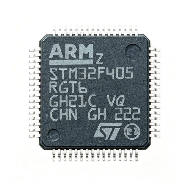
STM32F405RGT6 - MCU Cortex-M4F 168 MHz, 1 Mo de Flash | STMicroelectronics
Référence : STM32F405RGT6 ✓ Actif| Qté | Prix unitaire | Total |
|---|---|---|
| 1 | $11.5 | $11,50 |
| 10 | $10.2 | $102,00 |
| 100 | $8.85 | $885,00 |
| 500 | $7.6 | $3 800,00 |
| 1 000 | $6.75 | $6 750,00 |
STM32F405RGT6 Présentation
Un microcontrôleur (MCU) est un circuit intégré compact qui combine un cœur de processeur, de la mémoire volatile et non volatile, et des périphériques programmables sur une seule puce de silicium pour gouverner des opérations spécifiques dans les systèmes embarqués. Le STM32F405RGT6 appartient à la gamme de performance grand public STM32F4, qui s'inscrit dans la famille plus large des microcontrôleurs Flash 32 bits STM32. La hiérarchie des catégories est MCU -> MCU 32 bits -> MCU ARM Cortex-M -> MCU Cortex-M4 -> MCU STM32F4. Les MCU sont l'élément de contrôle central dans l'électronique industrielle, grand public, médicale et IoT.
Les caractéristiques principales incluent 3x CAN 12 bits (2,4 MSPS), 2x CNA 12 bits, 12x temporisateurs 16 bits plus 2x temporisateurs 32 bits, 51 GPIO, et une connectivité riche : 3x I2C, 4x USART plus 2x UART, 3x SPI, 2x CAN, USB 2.0 OTG Full-Speed et High-Speed avec PHY intégré, Ethernet 100 Mbit, SDIO, et une interface caméra DCMI. Le dispositif fonctionne de 1,8 V à 3,6 V et inclut un générateur de nombres aléatoires vrai, une unité CRC matérielle, et un identifiant unique de dispositif 96 bits.
Techniquement, la puce utilise un procédé CMOS 90 nm avec un ART Accelerator permettant une exécution sans état d'attente depuis la Flash, maximisant le débit effectif du Cortex-M4. Une unité de protection mémoire prend en charge une isolation robuste du firmware, tandis que plusieurs modes basse consommation (Sleep, Stop, Standby avec RTC) permettent l'optimisation énergétique pour les conceptions alimentées par batterie. Le PHY USB OTG HS intégré et le MAC Ethernet éliminent le coût BOM du PHY externe pour de nombreuses conceptions.
Les applications typiques incluent les entraînements moteur à contrôle vectoriel (servomoteurs FOC exploitant le FPU et les instructions DSP), la conversion de puissance numérique et les étages PFC, les automates PLC et contrôleurs d'automatisation industriels, les périphériques USB et dispositifs audio, et les produits grand public/médicaux nécessitant un traitement de signal en temps réel. L'écosystème open source STM32CubeIDE et STM32CubeMX avec bibliothèques HAL/LL raccourcit considérablement les cycles de développement.
Considération de conception : prévoir un découplage adéquat de 100 nF sur chaque paire de broches VDD/VSS, router les lignes USB HS D+/D- en paire différentielle 90 ohms, et maintenir les pistes SDIO de longueur égale. Noter également que des états d'attente Flash s'appliquent au-delà de 168 MHz si la configuration de l'ART Accelerator est modifiée.
Cette page synthétise les prix distributeurs, les alternatives compatibles vérifiées, et des notes de conception pratiques non consolidées dans la fiche technique du fabricant.
Alternatives de remplacement direct pour STM32F405RGT6 — même boîtier, compatible broche à broche. Les références à boîtier différent nécessitant une retouche du PCB sont exclues.
Variantes de cette série
Modèles de la même série directement compatibles avec STM32F405RGT6 (même facteur de forme et même empreinte) — différant par SRAM, ADC, Package, Timers, Flash Memory.
Outil de comparaison rapide — sélectionnez des références alternatives pour une comparaison côte à côte :
STM32F415RGT6
✓ En stock
$8.1 / unité
Voir la fiche technique →STM32F405ZGT6
✓ En stock
$8.1 / unité
Voir la fiche technique →STM32F405VGT6
✓ En stock
$8.1 / unité
Voir la fiche technique →STM32F407VGT6
✓ En stock
$7.55 / unité
Voir la fiche technique →STM32F405RGT7
📋 Alternative de référence (hors catalogue)
GD32F405RGT6
📋 Alternative de référence (hors catalogue)
STM32F405RGT6 Valeurs maximales et caractéristiques électriques
| Core | ARM Cortex-M4F (with single-precision FPU and DSP) |
| Fréquence d'horloge maximale | 168 MHz |
| Performance | 210 DMIPS (1.25 DMIPS/MHz) |
| Flash Memory | 1 MB (1M x 8) |
| SRAM | 192 KB (including 4 KB backup SRAM) |
| Operating Voltage | 1.8 V to 3.6 V |
| Boîtier | 64-LQFP (10x10 mm) |
| GPIO Count | 51 |
| ADC | 3x 12-bit, 2.4 MSPS, up to 24 channels |
| DAC | 2x 12-bit |
| Timers | 12x 16-bit + 2x 32-bit |
| Communication Interfaces | 3x I2C, 4x USART + 2x UART, 3x SPI, 2x CAN, USB OTG FS/HS, 100M Ethernet, SDIO, DCMI |
| Plage de température de fonctionnement | -40C to +85C |
| Type de montage | Surface Mount |
| Statut RoHS | Compliant |
| Lead-Free / Halogen-Free | Yes |
Configuration des broches de STM32F405RGT6
| Broche 1 | VBAT — Battery domain supply for RTC and backup SRAM |
| Broche 2 | PC13 — GPIO/Tamper-RTC (standard I/O with interrupt) |
| Broche 3 | PC14 — GPIO/OSC32_IN (32.768 kHz crystal) |
| Broche 4 | PC15 — GPIO/OSC32_OUT (32.768 kHz crystal) |
| Broche 5 | OSC_IN — HSE crystal/clock input |
| Broche 6 | OSC_OUT — HSE crystal output |
| Broche 7 | NRST — Reset input (active low) |
| Broche 8 | VSSA — Analog ground |
| Broche 9 | VDDA — Analog supply (1.8-3.6V) |
| Broche 10 | PA0-WKUP — GPIO/ADC0_IN0/Wakeup |
| Broche 11 | PA1 — GPIO/ADC0_IN1 |
| Broche 12 | PA2 — GPIO/USART2_TX/ADC0_IN2 |
| Broche 13 | PA3 — GPIO/USART2_RX/ADC0_IN3 |
| Broche 14 | PA4 — GPIO/SPI1_NSS/DAC_OUT1 |
| Broche 15 | PA5 — GPIO/SPI1_SCK/DAC_OUT2 |
| Broche 16 | PA6 — GPIO/SPI1_MISO/ADC1_IN2 |
| Broche 17 | PA7 — GPIO/SPI1_MOSI/ADC1_IN3 |
| Broche 18 | PB0 — GPIO/ADC2_IN8/TIM3_CH3 |
| Broche 19 | PB1 — GPIO/ADC2_IN9/TIM3_CH4 |
| Broche 20 | VSS_1 — Digital ground |
| Broche 21 | VDD_1 — Digital supply (1.8-3.6V) |
| Broche 22 | PB2/BOOT1 — GPIO/BOOT1 input |
| Broche 23 | PB10 — GPIO/I2C2_SCL/USART3_TX |
| Broche 24 | PB11 — GPIO/I2C2_SDA/USART3_RX |
| Broche 25 | VSS_2 — Digital ground |
| Broche 26 | VDD_2 — Digital supply (1.8-3.6V) |
| Broche 27 | PB12 — GPIO/SPI2_NSS/CAN2_RX |
| Broche 28 | PB13 — GPIO/SPI2_SCK/CAN2_TX |
| Broche 29 | PB14 — GPIO/SPI2_MISO/TIM12_CH1 |
| Broche 30 | PB15 — GPIO/SPI2_MOSI/TIM12_CH2 |
| Broche 31 | PA8 — GPIO/TIM1_CH1/USART1_CK/MCO |
| Broche 32 | PA9 — GPIO/USART1_TX/TIM1_CH2 |
| Broche 33 | PA10 — GPIO/USART1_RX/TIM1_CH3 |
| Broche 34 | PA11 — GPIO/USB_DM/CAN1_RX/TIM1_CH4 |
| Broche 35 | PA12 — GPIO/USB_DP/CAN1_TX/TIM1_ETR |
| Broche 36 | PA13 — GPIO/SWDIO |
| Broche 37 | VSS_3 — Digital ground |
| Broche 38 | VDD_3 — Digital supply (1.8-3.6V) |
| Broche 39 | PA14 — GPIO/SWCLK |
| Broche 40 | PA15 — GPIO/SPI3_NSS/TIM2_CH1 |
| Broche 41 | PC6 — GPIO/USART6_TX/TIM3_CH1 |
| Broche 42 | PC7 — GPIO/USART6_RX/TIM3_CH2 |
| Broche 43 | PC8 — GPIO/SDIO_D0/TIM3_CH3 |
| Broche 44 | PC9 — GPIO/SDIO_D1/TIM3_CH4 |
| Broche 45 | PA0 — GPIO/WKUP/USART2_CTS |
| Broche 46 | VDD_4 — Digital supply (1.8-3.6V) |
| Broche 47 | VSS_4 — Digital ground |
| Broche 48 | PB3 — GPIO/SPI3_SCK/TIM2_CH2 |
| Broche 49 | PB4 — GPIO/SPI3_MISO/TIM3_CH1 |
| Broche 50 | PB5 — GPIO/SPI3_MOSI/I2C1_SMBA |
| Broche 51 | PB6 — GPIO/I2C1_SCL/TIM4_CH1/USART1_TX |
| Broche 52 | PB7 — GPIO/I2C1_SDA/TIM4_CH2/USART1_RX |
| Broche 53 | BOOT0 — Boot mode select |
| Broche 54 | PB8 — GPIO/I2C1_SCL/CAN1_RX/TIM4_CH3 |
| Broche 55 | PB9 — GPIO/I2C1_SDA/CAN1_TX/TIM4_CH4 |
| Broche 56 | VSS_5 — Digital ground |
| Broche 57 | VDD_5 — Digital supply (1.8-3.6V) |
| Broche 58 | PD0 — GPIO/FSMC_D2/CAN1_RX |
| Broche 59 | PD1 — GPIO/FSMC_D3/CAN1_TX |
| Broche 60 | VREF+ — ADC positive reference |
| Broche 61 | VSSA — Analog ground |
| Broche 62 | VDDA — Analog supply |
| Broche 63 | PA13 — GPIO (secondary) |
| Broche 64 | VSS — Ground (additional) |
Applications typiques
STM32F405RGT6 convient pour 7 applications: Field-Oriented-Control Motor Drives, Industrial USB Host Peripherals, Digital Power Conversion and PFC, Audio Processing and DAC/ADC Interfaces, Industrial Ethernet Gateways, Consumer Medical Devices, Drones and Robotics Controllers.
Field-Oriented-Control Motor Drives
The STM32F405RGT6 fits FOC motor drives because the Cortex-M4F FPU and DSP instructions accelerate Park/Clarke transforms and PID loops by roughly 2-3x versus a Cortex-M3. The 168 MHz clock headroom leaves 30-40 percent CPU margin for encoder decoding and current-loop control. The 3x 12-bit ADCs sample phase currents at 2.4 MSPS, while the 12 timers provide complementary PWM with hardware dead-time insertion. Place a 100 nF decoupling cap on every VDD pin and route ADC inputs away from PWM switching nodes to preserve SNR.
Recommandé
Industrial USB Host Peripherals
The STM32F405RGT6 is widely used in industrial USB host peripherals because the integrated USB OTG Full-Speed and High-Speed PHY eliminates an external ULPI chip, reducing BOM by approximately USD 1-2. The Cortex-M4F core handles USB stack processing and application logic simultaneously. The SDIO controller and FSMC bus (on the F407 family variant) support external data buffering for printers, scanners, and data loggers. Designers should route the 90-ohm USB differential pair with length matching within 150 mil and add ESD protection diodes.
Recommandé
Digital Power Conversion and PFC
The STM32F405RGT6 is well-suited to digital power conversion and PFC stages because the Cortex-M4F single-precision FPU accelerates multiply-accumulate loops used in PID, state-space, and predictive control algorithms. The 12-bit ADCs sampled at 2.4 MSPS capture current and voltage waveforms with adequate bandwidth for PFC at 50-100 kHz switching. The high-resolution timer (217 ps) generates phase-shifted PWM for bridgeless PFC topologies. Plan 4-layer PCB layout to keep switching noise away from analog signal paths.
Recommandé
Audio Processing and DAC/ADC Interfaces
The STM32F405RGT6 serves audio processing applications because the Cortex-M4F SIMD instructions accelerate FFT, biquad, and dynamics processing at 48 kHz sample rates. The 2x 12-bit DACs and 3x 12-bit ADCs integrate codec functionality for budget audio products. The I2S-capable SPI port supports external 24-bit codecs. The 192 KB SRAM buffers multiple audio frames without external memory. Use DMA for both I2S RX and TX to keep the core free for DSP processing.
Recommandé
Industrial Ethernet Gateways
The STM32F405RGT6 fits industrial Ethernet gateways because the integrated 100 Mbit/s MAC and RMII interface connect to any standard Ethernet PHY for Modbus TCP, EtherNet/IP, or PROFINET. The Cortex-M4F core runs TCP/IP stacks plus application logic without external memory. The CAN 2.0B peripherals bridge fieldbus to enterprise networks. Pair with a wide-input DC-DC and provide 2 kV galvanic isolation on the Ethernet magnetics for industrial EMC compliance.
Recommandé
Consumer Medical Devices
The STM32F405RGT6 powers consumer medical devices like blood-pressure monitors, pulse oximeters, and spirometers because the Cortex-M4F core runs sensor-fusion DSP while the 12-bit ADC captures analog biosignals with 2.4 MSPS. The 1 MB Flash accommodates FDA-21CFR-Part-11 firmware with bootloader and OTA update. The USB OTG port provides powered device charging and data sync. Use the RTC with battery domain to maintain accurate timestamps across power cycles.
Recommandé
Drones and Robotics Controllers
The STM32F405RGT6 is a popular flight-controller MCU in hobbyist and commercial drones because the Cortex-M4F core runs Betaflight/Cleanflight/INAV firmware with full PID loops at 8 kHz update rates. The 168 MHz clock plus FPU computes quaternion math at rates that 72 MHz Cortex-M3 parts struggle to maintain. The 3x SPI ports connect to gyros, barometers, and radio receivers simultaneously. Mount the LQFP-64 with thermal vias to a copper pour for thermal relief at 50-60 mA active current.
Recommandé
Récapitulatif des produits recommandés
Données de référence d'ingénierie pour STM32F405RGT6 — comparaison, recommandations de conception et informations de conformité.
Guide de sélection
Comparaison avec les alternatives
| Paramètre | Ce produit | STM32F415RGT6 | STM32F405RGT7 | STM32F405ZGT6 | GD32F405RGT6 |
|---|---|---|---|---|---|
| Brand | STMicroelectronics | STMicroelectronics | STMicroelectronics | STMicroelectronics | GigaDevice |
| Package | 64-LQFP (10x10 mm) | 64-LQFP (10x10 mm) - same | 64-LQFP (10x10 mm) - same | 144-LQFP (20x20 mm) | 64-LQFP (10x10 mm) - same |
| Core | Cortex-M4F @ 168 MHz | Cortex-M4F @ 168 MHz | Cortex-M4F @ 168 MHz | Cortex-M4F @ 168 MHz | Cortex-M4F @ 168 MHz |
| Flash | 1 MB | 1 MB | 1 MB | 1 MB | 1 MB |
| SRAM | 192 KB | 192 KB | 192 KB | 192 KB | 192 KB |
| Crypto/Hash Engine | No | Yes (AES, SHA) | No | No | No |
| Operating Temperature | -40C to +85C | -40C to +85C | -40C to +105C | -40C to +85C | -40C to +85C |
| GPIO Count | 51 | 51 | 51 | 114 | 51 |
| Approx. Unit Price (1k qty) | USD 6.75 | USD 7.40 | USD 6.95 | USD 9.10 | USD 3.20 (GigaDevice, LCSC) |
Principaux différenciateurs
- PHY USB OTG High-Speed intégré (vs STM32F103RCT6 (Cortex-M3))
- FPU simple précision avec instructions DSP (vs STM32F103C8T6 (Cortex-M3))
- 1 Mo de Flash contre une base Cortex-M3 typique de 256-512 Ko (vs GD32F103RCT6)
Notes de conception
Prévoir un condensateur de découplage de 100 nF sur chaque paire de broches VDD/VSS, placé à moins de 2 mm de la broche. Ajouter un céramique de masse de 4,7 uF près du cluster VDD-1/VSS-1 et un tantale ou céramique de 10 uF à la sortie du régulateur. Pour le fonctionnement USB OTG HS, le PHY interne nécessite une alimentation VDD-USB stable à 90 pour cent de la valeur nominale avant l'activation de la PLL, sinon l'énumération échouera. Estimé : en supposant un courant actif de 100 mA à 3,3 V, la puissance totale est de 330 mW - le theta_JA du LQFP-64 d'environ 50 C/W donne une élévation de 16C au-dessus de l'ambiant, bien dans les limites de sécurité.
Router la paire USB OTG HS D+/D- en paire différentielle 90 ohms avec égalisation de longueur à 150 mil près et sans stubs. Garder les pistes du cristal courtes (moins de 5 mm) et les protéger par un plan de masse. Les signaux Ethernet RMII doivent être égalisés en longueur à 50 mil près par rapport au PHY externe. Les pistes SDIO doivent être égalisés en longueur à 100 mil près et routées sur la couche interne avec un plan de référence ininterrompu. Utiliser une pile 4 couches avec plan GND continu sous le MCU pour l'intégrité du chemin de retour.
Ne pas activer la PLL au-delà de 168 MHz sans confirmer la configuration des états d'attente Flash - zéro état d'attente n'est valide que jusqu'à 168 MHz. BOOT0 doit être tiré bas pour le démarrage Flash normal ou laissé flottant si non utilisé ; le laisser haut fait basculer le MCU dans le bootloader System Memory. Pour la précision ADC, s'assurer que VDDA est découplé avec une combinaison 100 nF + 1 uF et que VREF+ est contourné par un condensateur de 100 nF vers VSSA. Le pad exposé central du LQFP-64 (si présent) doit être soudé à un pad de masse pour la dissipation thermique.
Placer le cristal HSE à moins de 5 mm des broches OSC_IN/OSC_OUT avec des pistes courtes et symétriques. Router les signaux de débogage SWD/SWCLK à l'écart des nœuds de commutation à fort courant. Placer les résistances de tirage du mode boot et de reset à proximité du MCU. Prévoir un pad TEST sur PA13/PA14 pour la programmation en usine. La ligne NRST nécessite un condensateur de 100 nF plus une résistance de tirage de 10 kohm vers VDD et doit être exposée sur un connecteur pour la capacité de reset in-system.
Informations de conformité
RoHS compliant per ST product page. Not AEC-Q100 qualified; for automotive designs use the STM32F405RGT6-V variant or a different family member.


