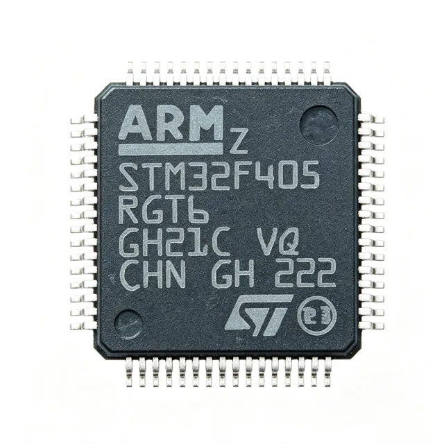
STM32F405RGT6 - MCU Cortex-M4F de 168MHz, 1MB de Flash | STMicroelectronics
N.º da peça: STM32F405RGT6 ✓ Ativo| Qtd. | Preço unitário | Total |
|---|---|---|
| 1 | $11.5 | $11,50 |
| 10 | $10.2 | $102,00 |
| 100 | $8.85 | $885,00 |
| 500 | $7.6 | $3.800,00 |
| 1.000 | $6.75 | $6.750,00 |
STM32F405RGT6 Visão geral
Um microcontrolador (MCU) é um circuito integrado compacto que combina um núcleo de processador, memória volátil e não volátil e periféricos programáveis em um único die de silício para governar operações específicas em sistemas embarcados. O STM32F405RGT6 pertence à linha de desempenho mainstream STM32F4, que está dentro da família mais ampla STM32 de microcontroladores Flash de 32 bits. A hierarquia de categorias é MCU -> MCU de 32 bits -> MCU ARM Cortex-M -> MCU Cortex-M4 -> MCU STM32F4. Os MCUs são o elemento de controle central em eletrônica industrial, de consumo, médica e de IoT.
Os principais recursos incluem 3x ADCs de 12 bits (2,4 MSPS), 2x DACs de 12 bits, 12x timers de 16 bits mais 2x timers de 32 bits, 51 GPIOs e conectividade rica: 3x I2C, 4x USART mais 2x UART, 3x SPI, 2x CAN, USB 2.0 OTG Full-Speed e High-Speed com PHY integrado, Ethernet de 100Mbit, SDIO e uma interface de câmera DCMI. O dispositivo opera de 1,8V a 3,6V e inclui um gerador de números aleatórios verdadeiro, unidade CRC de hardware e um ID único de dispositivo de 96 bits.
Tecnicamente, o chip usa um processo CMOS de 90 nm com um ART Accelerator que permite execução sem estados de espera a partir da Flash, maximizando a taxa de transferência efetiva do Cortex-M4. Uma unidade de proteção de memória suporta isolamento robusto de firmware, enquanto vários modos de baixo consumo (Sleep, Stop, Standby com RTC) permitem otimização de energia para projetos alimentados por bateria. O PHY USB OTG HS integrado e o MAC Ethernet eliminam o custo de BOM de PHY externo para muitos projetos.
Aplicações típicas incluem acionamentos de motor com controle orientado por campo (servoacionamentos FOC aproveitando a FPU e as instruções DSP), conversão de energia digital e estágios PFC, controladores PLC e de automação industrial, periféricos USB e dispositivos de áudio, e produtos de consumo/médicos que exigem processamento de sinais em tempo real. O ecossistema de código aberto STM32CubeIDE e STM32CubeMX com bibliotecas HAL/LL encurta significativamente os ciclos de desenvolvimento.
Consideração de projeto: forneça desacoplamento adequado de 100 nF em cada par de pinos VDD/VSS, roteie USB HS D+/D- como um par diferencial de 90 ohms e mantenha as trilhas SDIO com comprimentos casados. Observe também que estados de espera de Flash se aplicam acima de 168 MHz se a configuração do ART accelerator for alterada.
Esta página sintetiza preços de distribuidores, alternativas drop-in verificadas e notas práticas de projeto não consolidadas no datasheet do fabricante.
Alternativas drop-in para STM32F405RGT6 — mesmo encapsulamento, compatível pino a pino. Peças de encapsulamento diferente que exigem retrabalho na PCB são excluídas.
Variantes desta série
Modelos da mesma série compatíveis como drop-in com STM32F405RGT6 (mesmo formato e footprint) — diferindo em SRAM, Package, ADC, Timers, Flash Memory.
Ferramenta de comparação rápida — selecione peças alternativas para comparação lado a lado:
STM32F415RGT6
✓ Em estoque
$8.1 / unidade
Ver ficha técnica →STM32F405ZGT6
✓ Em estoque
$8.1 / unidade
Ver ficha técnica →STM32F405VGT6
✓ Em estoque
$8.1 / unidade
Ver ficha técnica →STM32F407VGT6
✓ Em estoque
$7.55 / unidade
Ver ficha técnica →STM32F405RGT7
✓ Em estoque
$7.95 / unidade
Ver ficha técnica →GD32F405RGT6
📋 Alternativa de referência (fora do catálogo)
STM32F405RGT6 Classificações máximas e características elétricas
| Core | ARM Cortex-M4F (with single-precision FPU and DSP) |
| Frequência máxima de clock | 168 MHz |
| Performance | 210 DMIPS (1.25 DMIPS/MHz) |
| Flash Memory | 1 MB (1M x 8) |
| SRAM | 192 KB (including 4 KB backup SRAM) |
| Operating Voltage | 1.8 V to 3.6 V |
| Encapsulamento | 64-LQFP (10x10 mm) |
| GPIO Count | 51 |
| ADC | 3x 12-bit, 2.4 MSPS, up to 24 channels |
| DAC | 2x 12-bit |
| Timers | 12x 16-bit + 2x 32-bit |
| Communication Interfaces | 3x I2C, 4x USART + 2x UART, 3x SPI, 2x CAN, USB OTG FS/HS, 100M Ethernet, SDIO, DCMI |
| Faixa de temperatura de operação | -40C to +85C |
| Tipo de montagem | Surface Mount |
| Status RoHS | Compliant |
| Lead-Free / Halogen-Free | Yes |
Configuração de pinos do STM32F405RGT6
| Pino 1 | VBAT — Battery domain supply for RTC and backup SRAM |
| Pino 2 | PC13 — GPIO/Tamper-RTC (standard I/O with interrupt) |
| Pino 3 | PC14 — GPIO/OSC32_IN (32.768 kHz crystal) |
| Pino 4 | PC15 — GPIO/OSC32_OUT (32.768 kHz crystal) |
| Pino 5 | OSC_IN — HSE crystal/clock input |
| Pino 6 | OSC_OUT — HSE crystal output |
| Pino 7 | NRST — Reset input (active low) |
| Pino 8 | VSSA — Analog ground |
| Pino 9 | VDDA — Analog supply (1.8-3.6V) |
| Pino 10 | PA0-WKUP — GPIO/ADC0_IN0/Wakeup |
| Pino 11 | PA1 — GPIO/ADC0_IN1 |
| Pino 12 | PA2 — GPIO/USART2_TX/ADC0_IN2 |
| Pino 13 | PA3 — GPIO/USART2_RX/ADC0_IN3 |
| Pino 14 | PA4 — GPIO/SPI1_NSS/DAC_OUT1 |
| Pino 15 | PA5 — GPIO/SPI1_SCK/DAC_OUT2 |
| Pino 16 | PA6 — GPIO/SPI1_MISO/ADC1_IN2 |
| Pino 17 | PA7 — GPIO/SPI1_MOSI/ADC1_IN3 |
| Pino 18 | PB0 — GPIO/ADC2_IN8/TIM3_CH3 |
| Pino 19 | PB1 — GPIO/ADC2_IN9/TIM3_CH4 |
| Pino 20 | VSS_1 — Digital ground |
| Pino 21 | VDD_1 — Digital supply (1.8-3.6V) |
| Pino 22 | PB2/BOOT1 — GPIO/BOOT1 input |
| Pino 23 | PB10 — GPIO/I2C2_SCL/USART3_TX |
| Pino 24 | PB11 — GPIO/I2C2_SDA/USART3_RX |
| Pino 25 | VSS_2 — Digital ground |
| Pino 26 | VDD_2 — Digital supply (1.8-3.6V) |
| Pino 27 | PB12 — GPIO/SPI2_NSS/CAN2_RX |
| Pino 28 | PB13 — GPIO/SPI2_SCK/CAN2_TX |
| Pino 29 | PB14 — GPIO/SPI2_MISO/TIM12_CH1 |
| Pino 30 | PB15 — GPIO/SPI2_MOSI/TIM12_CH2 |
| Pino 31 | PA8 — GPIO/TIM1_CH1/USART1_CK/MCO |
| Pino 32 | PA9 — GPIO/USART1_TX/TIM1_CH2 |
| Pino 33 | PA10 — GPIO/USART1_RX/TIM1_CH3 |
| Pino 34 | PA11 — GPIO/USB_DM/CAN1_RX/TIM1_CH4 |
| Pino 35 | PA12 — GPIO/USB_DP/CAN1_TX/TIM1_ETR |
| Pino 36 | PA13 — GPIO/SWDIO |
| Pino 37 | VSS_3 — Digital ground |
| Pino 38 | VDD_3 — Digital supply (1.8-3.6V) |
| Pino 39 | PA14 — GPIO/SWCLK |
| Pino 40 | PA15 — GPIO/SPI3_NSS/TIM2_CH1 |
| Pino 41 | PC6 — GPIO/USART6_TX/TIM3_CH1 |
| Pino 42 | PC7 — GPIO/USART6_RX/TIM3_CH2 |
| Pino 43 | PC8 — GPIO/SDIO_D0/TIM3_CH3 |
| Pino 44 | PC9 — GPIO/SDIO_D1/TIM3_CH4 |
| Pino 45 | PA0 — GPIO/WKUP/USART2_CTS |
| Pino 46 | VDD_4 — Digital supply (1.8-3.6V) |
| Pino 47 | VSS_4 — Digital ground |
| Pino 48 | PB3 — GPIO/SPI3_SCK/TIM2_CH2 |
| Pino 49 | PB4 — GPIO/SPI3_MISO/TIM3_CH1 |
| Pino 50 | PB5 — GPIO/SPI3_MOSI/I2C1_SMBA |
| Pino 51 | PB6 — GPIO/I2C1_SCL/TIM4_CH1/USART1_TX |
| Pino 52 | PB7 — GPIO/I2C1_SDA/TIM4_CH2/USART1_RX |
| Pino 53 | BOOT0 — Boot mode select |
| Pino 54 | PB8 — GPIO/I2C1_SCL/CAN1_RX/TIM4_CH3 |
| Pino 55 | PB9 — GPIO/I2C1_SDA/CAN1_TX/TIM4_CH4 |
| Pino 56 | VSS_5 — Digital ground |
| Pino 57 | VDD_5 — Digital supply (1.8-3.6V) |
| Pino 58 | PD0 — GPIO/FSMC_D2/CAN1_RX |
| Pino 59 | PD1 — GPIO/FSMC_D3/CAN1_TX |
| Pino 60 | VREF+ — ADC positive reference |
| Pino 61 | VSSA — Analog ground |
| Pino 62 | VDDA — Analog supply |
| Pino 63 | PA13 — GPIO (secondary) |
| Pino 64 | VSS — Ground (additional) |
Aplicações típicas
STM32F405RGT6 é adequado para 7 aplicaçãos: Field-Oriented-Control Motor Drives, Industrial USB Host Peripherals, Digital Power Conversion and PFC, Audio Processing and DAC/ADC Interfaces, Industrial Ethernet Gateways, Consumer Medical Devices, Drones and Robotics Controllers.
Field-Oriented-Control Motor Drives
The STM32F405RGT6 fits FOC motor drives because the Cortex-M4F FPU and DSP instructions accelerate Park/Clarke transforms and PID loops by roughly 2-3x versus a Cortex-M3. The 168 MHz clock headroom leaves 30-40 percent CPU margin for encoder decoding and current-loop control. The 3x 12-bit ADCs sample phase currents at 2.4 MSPS, while the 12 timers provide complementary PWM with hardware dead-time insertion. Place a 100 nF decoupling cap on every VDD pin and route ADC inputs away from PWM switching nodes to preserve SNR.
Recomendado
Industrial USB Host Peripherals
The STM32F405RGT6 is widely used in industrial USB host peripherals because the integrated USB OTG Full-Speed and High-Speed PHY eliminates an external ULPI chip, reducing BOM by approximately USD 1-2. The Cortex-M4F core handles USB stack processing and application logic simultaneously. The SDIO controller and FSMC bus (on the F407 family variant) support external data buffering for printers, scanners, and data loggers. Designers should route the 90-ohm USB differential pair with length matching within 150 mil and add ESD protection diodes.
Recomendado
Digital Power Conversion and PFC
The STM32F405RGT6 is well-suited to digital power conversion and PFC stages because the Cortex-M4F single-precision FPU accelerates multiply-accumulate loops used in PID, state-space, and predictive control algorithms. The 12-bit ADCs sampled at 2.4 MSPS capture current and voltage waveforms with adequate bandwidth for PFC at 50-100 kHz switching. The high-resolution timer (217 ps) generates phase-shifted PWM for bridgeless PFC topologies. Plan 4-layer PCB layout to keep switching noise away from analog signal paths.
Recomendado
Audio Processing and DAC/ADC Interfaces
The STM32F405RGT6 serves audio processing applications because the Cortex-M4F SIMD instructions accelerate FFT, biquad, and dynamics processing at 48 kHz sample rates. The 2x 12-bit DACs and 3x 12-bit ADCs integrate codec functionality for budget audio products. The I2S-capable SPI port supports external 24-bit codecs. The 192 KB SRAM buffers multiple audio frames without external memory. Use DMA for both I2S RX and TX to keep the core free for DSP processing.
Recomendado
Industrial Ethernet Gateways
The STM32F405RGT6 fits industrial Ethernet gateways because the integrated 100 Mbit/s MAC and RMII interface connect to any standard Ethernet PHY for Modbus TCP, EtherNet/IP, or PROFINET. The Cortex-M4F core runs TCP/IP stacks plus application logic without external memory. The CAN 2.0B peripherals bridge fieldbus to enterprise networks. Pair with a wide-input DC-DC and provide 2 kV galvanic isolation on the Ethernet magnetics for industrial EMC compliance.
Recomendado
Consumer Medical Devices
The STM32F405RGT6 powers consumer medical devices like blood-pressure monitors, pulse oximeters, and spirometers because the Cortex-M4F core runs sensor-fusion DSP while the 12-bit ADC captures analog biosignals with 2.4 MSPS. The 1 MB Flash accommodates FDA-21CFR-Part-11 firmware with bootloader and OTA update. The USB OTG port provides powered device charging and data sync. Use the RTC with battery domain to maintain accurate timestamps across power cycles.
Recomendado
Drones and Robotics Controllers
The STM32F405RGT6 is a popular flight-controller MCU in hobbyist and commercial drones because the Cortex-M4F core runs Betaflight/Cleanflight/INAV firmware with full PID loops at 8 kHz update rates. The 168 MHz clock plus FPU computes quaternion math at rates that 72 MHz Cortex-M3 parts struggle to maintain. The 3x SPI ports connect to gyros, barometers, and radio receivers simultaneously. Mount the LQFP-64 with thermal vias to a copper pour for thermal relief at 50-60 mA active current.
Recomendado
Resumo dos produtos recomendados
Dados de referência de engenharia para STM32F405RGT6 — comparação, orientação de projeto e informações de conformidade.
Guia de seleção
Comparação com alternativas
| Parâmetro | Este produto | STM32F415RGT6 | STM32F405RGT7 | STM32F405ZGT6 | GD32F405RGT6 |
|---|---|---|---|---|---|
| Brand | STMicroelectronics | STMicroelectronics | STMicroelectronics | STMicroelectronics | GigaDevice |
| Package | 64-LQFP (10x10 mm) | 64-LQFP (10x10 mm) - same | 64-LQFP (10x10 mm) - same | 144-LQFP (20x20 mm) | 64-LQFP (10x10 mm) - same |
| Core | Cortex-M4F @ 168 MHz | Cortex-M4F @ 168 MHz | Cortex-M4F @ 168 MHz | Cortex-M4F @ 168 MHz | Cortex-M4F @ 168 MHz |
| Flash | 1 MB | 1 MB | 1 MB | 1 MB | 1 MB |
| SRAM | 192 KB | 192 KB | 192 KB | 192 KB | 192 KB |
| Crypto/Hash Engine | No | Yes (AES, SHA) | No | No | No |
| Operating Temperature | -40C to +85C | -40C to +85C | -40C to +105C | -40C to +85C | -40C to +85C |
| GPIO Count | 51 | 51 | 51 | 114 | 51 |
| Approx. Unit Price (1k qty) | USD 6.75 | USD 7.40 | USD 6.95 | USD 9.10 | USD 3.20 (GigaDevice, LCSC) |
Principais diferenciais
- PHY USB OTG High-Speed integrado (vs STM32F103RCT6 (Cortex-M3))
- FPU de precisão simples com instruções DSP (vs STM32F103C8T6 (Cortex-M3))
- 1 MB de Flash versus linha de base típica de 256-512 KB Cortex-M3 (vs GD32F103RCT6)
Notas de projeto
Forneça um capacitor de desacoplamento de 100 nF em cada par de pinos VDD/VSS, posicionado a menos de 2 mm do pino. Adicione um cerâmico bulk de 4,7 uF próximo ao cluster VDD-1/VSS-1 e um tântalo ou cerâmico de 10 uF na saída do regulador. Para operação USB OTG HS, o PHY interno requer alimentação VDD-USB estável dentro de 90 por cento do nominal antes de habilitar o PLL, caso contrário a enumeração falhará. Estimado: assumindo corrente ativa de 100 mA em 3,3V, a potência total é 330 mW - o theta_JA do LQFP-64 de aproximadamente 50 C/W resulta em elevação de 16C acima da ambiente, bem dentro de limites seguros.
Roteie o par USB OTG HS D+/D- como um par diferencial de 90 ohms com comprimentos casados dentro de 150 mil e sem stubs. Mantenha as trilhas do cristal curtas (menos de 5 mm) e proteja-as com um plano de terra. Os sinais Ethernet RMII devem ter comprimentos casados dentro de 50 mil em relação ao PHY externo. As trilhas SDIO devem ter comprimentos casados dentro de 100 mil e ser roteadas na camada interna com um plano de referência ininterrupto. Use stackup de 4 camadas com plano GND contínuo sob o MCU para integridade do caminho de retorno.
Não habilite o PLL acima de 168 MHz sem confirmar a configuração de estados de espera da Flash - zero estados de espera só é válido até 168 MHz. BOOT0 deve ser puxado para baixo para boot normal da Flash ou deixado flutuando se não usado; deixá-lo alto coloca o MCU no bootloader de System Memory. Para precisão do ADC, garanta que VDDA seja desacoplado com uma combinação de 100 nF + 1 uF e que VREF+ seja bypassado com um capacitor de 100 nF para VSSA. O pad exposto central do LQFP-64 (se presente) deve ser soldado a um pad de terra para alívio térmico.
Posicione o cristal HSE a menos de 5 mm dos pinos OSC_IN/OSC_OUT com trilhas curtas e simétricas. Roteie os sinais de depuração SWD/SWCLK longe de nós de chaveamento de alta corrente. Posicione os pull-ups de modo de boot e reset adjacentes ao MCU. Forneça um pad TEST em PA13/PA14 para programação de fábrica. A linha NRST precisa de um capacitor de 100 nF mais pull-up de 10 kohm para VDD e deve ser exposta em um header para capacidade de reset in-system.
Informações de conformidade
RoHS compliant per ST product page. Not AEC-Q100 qualified; for automotive designs use the STM32F405RGT6-V variant or a different family member.


