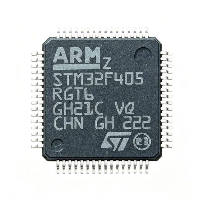
STM32F405RGT6 - 168MHz Cortex-M4F、1MBフラッシュMCU | STMicroelectronics
部品番号: STM32F405RGT6 ✓ 生産中| 数量 | 単価 | 小計 |
|---|---|---|
| 1 | $11.5 | $11.50 |
| 10 | $10.2 | $102.00 |
| 100 | $8.85 | $885.00 |
| 500 | $7.6 | $3,800.00 |
| 1,000 | $6.75 | $6,750.00 |
STM32F405RGT6 概要
マイクロコントローラ(MCU)は、プロセッサコア、揮発性・不揮発性メモリ、およびプログラマブルペリフェラルを単一のシリコンダイ上に統合し、組み込みシステムの特定の動作を制御する小型集積回路です。STM32F405RGT6は、32ビットフラッシュマイクロコントローラの広範なSTM32ファミリ内に位置するSTM32F4メインストリーム性能ラインに属します。カテゴリ階層はMCU -> 32ビットMCU -> ARM Cortex-M MCU -> Cortex-M4 MCU -> STM32F4 MCUです。MCUは産業、民生、医療、IoTエレクトロニクスにおける中心的な制御要素です。
主な機能には、3x 12ビットADC(2.4 MSPS)、2x 12ビットDAC、12x 16ビットタイマ+2x 32ビットタイマ、51 GPIO、および豊富な接続性(3x I2C、4x USART+2x UART、3x SPI、2x CAN、オンチップPHY付きUSB 2.0 OTG Full-Speed/High-Speed、100Mbit Ethernet、SDIO、DCMIカメラインターフェース)が含まれます。デバイスは1.8V~3.6Vで動作し、真の乱数生成器、ハードウェアCRCユニット、96ビットのユニークデバイスIDを備えています。
技術的には、このチップは90 nm CMOSプロセスを使用し、ARTアクセラレータによりフラッシュからのゼロウェイトステート実行を可能にし、Cortex-M4の実効スループットを最大化します。メモリ保護ユニットは堅牢なファームウェア分離をサポートし、複数の低電力モード(Sleep、Stop、RTC付きStandby)によりバッテリ駆動設計のエネルギー最適化が可能です。統合されたUSB OTG HS PHYとEthernet MACにより、多くの設計で外部PHYのBOMコストが不要になります。
代表的なアプリケーションには、フィールドオリエンテッド制御モータドライブ(FPUとDSP命令を活用したFOCサーボドライブ)、デジタル電源変換およびPFC段、産業用PLCおよび自動化コントローラ、USBペリフェラルおよびオーディオデバイス、リアルタイム信号処理を必要とする民生/医療製品が含まれます。オープンソースのSTM32CubeIDEおよびSTM32CubeMXエコシステムとHAL/LLライブラリにより、開発サイクルが大幅に短縮されます。
設計上の考慮事項:すべてのVDD/VSSピンペアに十分な100 nFデカップリングを設け、USB HS D+/D-を90オーム差動ペアとして配線し、SDIOトレースの長さを整合させてください。また、ARTアクセラレータの設定を変更した場合、168MHzを超えるとフラッシュウェイトステートが適用されることに注意してください。
このページは、ディストリビュータ価格、検証済みのドロップイン代替品、およびメーカーデータシートに統合されていない実用的な設計ノートをまとめたものです。
ドロップイン代替品: STM32F405RGT6 — 同一パッケージでピン互換。PCBの作り直しが必要な異なるパッケージの部品は除外されています。
このシリーズのバリエーション
同一シリーズでドロップイン互換のモデル: STM32F405RGT6 (同一形状・フットプリント) — 相違点: SRAM, Package, ADC, Timers, Flash Memory.
クイック比較ツール — 並列比較する代替部品を選択:
STM32F415RGT6
✓ 在庫あり
$8.1 / 個
データシートを見る →STM32F405ZGT6
✓ 在庫あり
$8.1 / 個
データシートを見る →STM32F405VGT6
✓ 在庫あり
$8.1 / 個
データシートを見る →STM32F407VGT6
✓ 在庫あり
$7.55 / 個
データシートを見る →STM32F405RGT7
✓ 在庫あり
$7.95 / 個
データシートを見る →GD32F405RGT6
📋 参考代替品(カタログ未掲載)
STM32F405RGT6 最大定格&電気的特性
| Core | ARM Cortex-M4F (with single-precision FPU and DSP) |
| 最大クロック周波数 | 168 MHz |
| Performance | 210 DMIPS (1.25 DMIPS/MHz) |
| Flash Memory | 1 MB (1M x 8) |
| SRAM | 192 KB (including 4 KB backup SRAM) |
| Operating Voltage | 1.8 V to 3.6 V |
| パッケージ | 64-LQFP (10x10 mm) |
| GPIO Count | 51 |
| ADC | 3x 12-bit, 2.4 MSPS, up to 24 channels |
| DAC | 2x 12-bit |
| Timers | 12x 16-bit + 2x 32-bit |
| Communication Interfaces | 3x I2C, 4x USART + 2x UART, 3x SPI, 2x CAN, USB OTG FS/HS, 100M Ethernet, SDIO, DCMI |
| 動作温度範囲 | -40C to +85C |
| 実装タイプ | Surface Mount |
| RoHS ステータス | Compliant |
| Lead-Free / Halogen-Free | Yes |
STM32F405RGT6 ピン構成
| ピン 1 | VBAT — Battery domain supply for RTC and backup SRAM |
| ピン 2 | PC13 — GPIO/Tamper-RTC (standard I/O with interrupt) |
| ピン 3 | PC14 — GPIO/OSC32_IN (32.768 kHz crystal) |
| ピン 4 | PC15 — GPIO/OSC32_OUT (32.768 kHz crystal) |
| ピン 5 | OSC_IN — HSE crystal/clock input |
| ピン 6 | OSC_OUT — HSE crystal output |
| ピン 7 | NRST — Reset input (active low) |
| ピン 8 | VSSA — Analog ground |
| ピン 9 | VDDA — Analog supply (1.8-3.6V) |
| ピン 10 | PA0-WKUP — GPIO/ADC0_IN0/Wakeup |
| ピン 11 | PA1 — GPIO/ADC0_IN1 |
| ピン 12 | PA2 — GPIO/USART2_TX/ADC0_IN2 |
| ピン 13 | PA3 — GPIO/USART2_RX/ADC0_IN3 |
| ピン 14 | PA4 — GPIO/SPI1_NSS/DAC_OUT1 |
| ピン 15 | PA5 — GPIO/SPI1_SCK/DAC_OUT2 |
| ピン 16 | PA6 — GPIO/SPI1_MISO/ADC1_IN2 |
| ピン 17 | PA7 — GPIO/SPI1_MOSI/ADC1_IN3 |
| ピン 18 | PB0 — GPIO/ADC2_IN8/TIM3_CH3 |
| ピン 19 | PB1 — GPIO/ADC2_IN9/TIM3_CH4 |
| ピン 20 | VSS_1 — Digital ground |
| ピン 21 | VDD_1 — Digital supply (1.8-3.6V) |
| ピン 22 | PB2/BOOT1 — GPIO/BOOT1 input |
| ピン 23 | PB10 — GPIO/I2C2_SCL/USART3_TX |
| ピン 24 | PB11 — GPIO/I2C2_SDA/USART3_RX |
| ピン 25 | VSS_2 — Digital ground |
| ピン 26 | VDD_2 — Digital supply (1.8-3.6V) |
| ピン 27 | PB12 — GPIO/SPI2_NSS/CAN2_RX |
| ピン 28 | PB13 — GPIO/SPI2_SCK/CAN2_TX |
| ピン 29 | PB14 — GPIO/SPI2_MISO/TIM12_CH1 |
| ピン 30 | PB15 — GPIO/SPI2_MOSI/TIM12_CH2 |
| ピン 31 | PA8 — GPIO/TIM1_CH1/USART1_CK/MCO |
| ピン 32 | PA9 — GPIO/USART1_TX/TIM1_CH2 |
| ピン 33 | PA10 — GPIO/USART1_RX/TIM1_CH3 |
| ピン 34 | PA11 — GPIO/USB_DM/CAN1_RX/TIM1_CH4 |
| ピン 35 | PA12 — GPIO/USB_DP/CAN1_TX/TIM1_ETR |
| ピン 36 | PA13 — GPIO/SWDIO |
| ピン 37 | VSS_3 — Digital ground |
| ピン 38 | VDD_3 — Digital supply (1.8-3.6V) |
| ピン 39 | PA14 — GPIO/SWCLK |
| ピン 40 | PA15 — GPIO/SPI3_NSS/TIM2_CH1 |
| ピン 41 | PC6 — GPIO/USART6_TX/TIM3_CH1 |
| ピン 42 | PC7 — GPIO/USART6_RX/TIM3_CH2 |
| ピン 43 | PC8 — GPIO/SDIO_D0/TIM3_CH3 |
| ピン 44 | PC9 — GPIO/SDIO_D1/TIM3_CH4 |
| ピン 45 | PA0 — GPIO/WKUP/USART2_CTS |
| ピン 46 | VDD_4 — Digital supply (1.8-3.6V) |
| ピン 47 | VSS_4 — Digital ground |
| ピン 48 | PB3 — GPIO/SPI3_SCK/TIM2_CH2 |
| ピン 49 | PB4 — GPIO/SPI3_MISO/TIM3_CH1 |
| ピン 50 | PB5 — GPIO/SPI3_MOSI/I2C1_SMBA |
| ピン 51 | PB6 — GPIO/I2C1_SCL/TIM4_CH1/USART1_TX |
| ピン 52 | PB7 — GPIO/I2C1_SDA/TIM4_CH2/USART1_RX |
| ピン 53 | BOOT0 — Boot mode select |
| ピン 54 | PB8 — GPIO/I2C1_SCL/CAN1_RX/TIM4_CH3 |
| ピン 55 | PB9 — GPIO/I2C1_SDA/CAN1_TX/TIM4_CH4 |
| ピン 56 | VSS_5 — Digital ground |
| ピン 57 | VDD_5 — Digital supply (1.8-3.6V) |
| ピン 58 | PD0 — GPIO/FSMC_D2/CAN1_RX |
| ピン 59 | PD1 — GPIO/FSMC_D3/CAN1_TX |
| ピン 60 | VREF+ — ADC positive reference |
| ピン 61 | VSSA — Analog ground |
| ピン 62 | VDDA — Analog supply |
| ピン 63 | PA13 — GPIO (secondary) |
| ピン 64 | VSS — Ground (additional) |
主な用途
STM32F405RGT6 の用途: 7 件s: Field-Oriented-Control Motor Drives, Industrial USB Host Peripherals, Digital Power Conversion and PFC, Audio Processing and DAC/ADC Interfaces, Industrial Ethernet Gateways, Consumer Medical Devices, Drones and Robotics Controllers.
Field-Oriented-Control Motor Drives
The STM32F405RGT6 fits FOC motor drives because the Cortex-M4F FPU and DSP instructions accelerate Park/Clarke transforms and PID loops by roughly 2-3x versus a Cortex-M3. The 168 MHz clock headroom leaves 30-40 percent CPU margin for encoder decoding and current-loop control. The 3x 12-bit ADCs sample phase currents at 2.4 MSPS, while the 12 timers provide complementary PWM with hardware dead-time insertion. Place a 100 nF decoupling cap on every VDD pin and route ADC inputs away from PWM switching nodes to preserve SNR.
おすすめ
Industrial USB Host Peripherals
The STM32F405RGT6 is widely used in industrial USB host peripherals because the integrated USB OTG Full-Speed and High-Speed PHY eliminates an external ULPI chip, reducing BOM by approximately USD 1-2. The Cortex-M4F core handles USB stack processing and application logic simultaneously. The SDIO controller and FSMC bus (on the F407 family variant) support external data buffering for printers, scanners, and data loggers. Designers should route the 90-ohm USB differential pair with length matching within 150 mil and add ESD protection diodes.
おすすめ
Digital Power Conversion and PFC
The STM32F405RGT6 is well-suited to digital power conversion and PFC stages because the Cortex-M4F single-precision FPU accelerates multiply-accumulate loops used in PID, state-space, and predictive control algorithms. The 12-bit ADCs sampled at 2.4 MSPS capture current and voltage waveforms with adequate bandwidth for PFC at 50-100 kHz switching. The high-resolution timer (217 ps) generates phase-shifted PWM for bridgeless PFC topologies. Plan 4-layer PCB layout to keep switching noise away from analog signal paths.
おすすめ
Audio Processing and DAC/ADC Interfaces
The STM32F405RGT6 serves audio processing applications because the Cortex-M4F SIMD instructions accelerate FFT, biquad, and dynamics processing at 48 kHz sample rates. The 2x 12-bit DACs and 3x 12-bit ADCs integrate codec functionality for budget audio products. The I2S-capable SPI port supports external 24-bit codecs. The 192 KB SRAM buffers multiple audio frames without external memory. Use DMA for both I2S RX and TX to keep the core free for DSP processing.
おすすめ
Industrial Ethernet Gateways
The STM32F405RGT6 fits industrial Ethernet gateways because the integrated 100 Mbit/s MAC and RMII interface connect to any standard Ethernet PHY for Modbus TCP, EtherNet/IP, or PROFINET. The Cortex-M4F core runs TCP/IP stacks plus application logic without external memory. The CAN 2.0B peripherals bridge fieldbus to enterprise networks. Pair with a wide-input DC-DC and provide 2 kV galvanic isolation on the Ethernet magnetics for industrial EMC compliance.
おすすめ
Consumer Medical Devices
The STM32F405RGT6 powers consumer medical devices like blood-pressure monitors, pulse oximeters, and spirometers because the Cortex-M4F core runs sensor-fusion DSP while the 12-bit ADC captures analog biosignals with 2.4 MSPS. The 1 MB Flash accommodates FDA-21CFR-Part-11 firmware with bootloader and OTA update. The USB OTG port provides powered device charging and data sync. Use the RTC with battery domain to maintain accurate timestamps across power cycles.
おすすめ
Drones and Robotics Controllers
The STM32F405RGT6 is a popular flight-controller MCU in hobbyist and commercial drones because the Cortex-M4F core runs Betaflight/Cleanflight/INAV firmware with full PID loops at 8 kHz update rates. The 168 MHz clock plus FPU computes quaternion math at rates that 72 MHz Cortex-M3 parts struggle to maintain. The 3x SPI ports connect to gyros, barometers, and radio receivers simultaneously. Mount the LQFP-64 with thermal vias to a copper pour for thermal relief at 50-60 mA active current.
おすすめ
おすすめ製品の概要
エンジニアリング参考データ: STM32F405RGT6 — 比較、設計ガイダンス、コンプライアンス情報。
選定ガイド
代替品との比較
| パラメータ | この製品 | STM32F415RGT6 | STM32F405RGT7 | STM32F405ZGT6 | GD32F405RGT6 |
|---|---|---|---|---|---|
| Brand | STMicroelectronics | STMicroelectronics | STMicroelectronics | STMicroelectronics | GigaDevice |
| Package | 64-LQFP (10x10 mm) | 64-LQFP (10x10 mm) - same | 64-LQFP (10x10 mm) - same | 144-LQFP (20x20 mm) | 64-LQFP (10x10 mm) - same |
| Core | Cortex-M4F @ 168 MHz | Cortex-M4F @ 168 MHz | Cortex-M4F @ 168 MHz | Cortex-M4F @ 168 MHz | Cortex-M4F @ 168 MHz |
| Flash | 1 MB | 1 MB | 1 MB | 1 MB | 1 MB |
| SRAM | 192 KB | 192 KB | 192 KB | 192 KB | 192 KB |
| Crypto/Hash Engine | No | Yes (AES, SHA) | No | No | No |
| Operating Temperature | -40C to +85C | -40C to +85C | -40C to +105C | -40C to +85C | -40C to +85C |
| GPIO Count | 51 | 51 | 51 | 114 | 51 |
| Approx. Unit Price (1k qty) | USD 6.75 | USD 7.40 | USD 6.95 | USD 9.10 | USD 3.20 (GigaDevice, LCSC) |
主な差別化要因
- 統合USB OTG High-Speed PHY (vs STM32F103RCT6(Cortex-M3))
- DSP命令付き単精度FPU (vs STM32F103C8T6(Cortex-M3))
- 1 MBフラッシュ対一般的な256-512 KB Cortex-M3ベースライン (vs GD32F103RCT6)
設計ノート
すべてのVDD/VSSピンペアに100 nFデカップリングコンデンサを設け、ピンから2 mm以内に配置してください。VDD-1/VSS-1クラスタ近傍に4.7 uFセラミックのバルクコンデンサを追加し、レギュレータ出力に10 uFタンタルまたはセラミックを配置してください。USB OTG HS動作では、内部PHYはPLL有効化前にVDD-USB電源が公称値の90パーセント以内で安定している必要があり、そうでないとエニュメレーションが失敗します。推定:3.3Vで100 mAのアクティブ電流を仮定すると、総消費電力は330 mWです。LQFP-64のtheta_JAは約50 C/Wで、周囲温度より16C上昇しますが、安全限界内です。
USB OTG HS D+/D-ペアを90オーム差動ペアとして配線し、長さを150 mil以内で整合させ、スタブを設けないでください。水晶トレースは短く(5 mm未満)保ち、グランドプレーンでガードしてください。Ethernet RMII信号は外部PHYに対して50 mil以内で長さを整合させる必要があります。SDIOトレースは100 mil以内で長さを整合させ、途切れのないリファレンスプレーンを持つ内層に配線してください。リターンパスの整合性のために、MCU下に連続したGNDプレーンを持つ4層スタックアップを使用してください。
フラッシュウェイトステート設定を確認せずに168MHzを超えてPLLを有効にしないでください。ゼロウェイトステートは168MHzまでのみ有効です。BOOT0は通常のフラッシュブートではLowにプルダウンするか、未使用の場合はフローティングにしてください。HighのままにするとMCUはシステムメモリブートローダに入ります。ADC精度のために、VDDAを100 nF+1 uFの組み合わせでデカップリングし、VREF+を100 nFコンデンサでVSSAにバイパスしてください。LQFP-64の中央露出パッド(存在する場合)は、熱放散のためにグランドパッドにはんだ付けする必要があります。
HSE水晶をOSC_IN/OSC_OUTピンから5 mm以内に配置し、短く対称なトレースにしてください。SWD/SWCLKデバッグ信号を大電流スイッチングノードから遠ざけて配線してください。ブートモードおよびリセットのプルアップをMCUの近傍に配置してください。工場プログラミング用にPA13/PA14にTESTパッドを設けてください。NRSTラインには100 nFコンデンサと10 kohmのVDDへのプルアップが必要で、インシステムリセット機能のためにヘッダに露出させる必要があります。
コンプライアンス情報
RoHS compliant per ST product page. Not AEC-Q100 qualified; for automotive designs use the STM32F405RGT6-V variant or a different family member.


