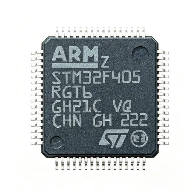
STM32F405RGT6 – 168 MHz Cortex-M4F, 1 MB Flash MCU | STMicroelectronics
Teilenummer: STM32F405RGT6 ✓ Aktiv| Menge | Stückpreis | Gesamt |
|---|---|---|
| 1 | $11.5 | $11,50 |
| 10 | $10.2 | $102,00 |
| 100 | $8.85 | $885,00 |
| 500 | $7.6 | $3.800,00 |
| 1.000 | $6.75 | $6.750,00 |
STM32F405RGT6 Übersicht
Ein Mikrocontroller (MCU) ist eine kompakte integrierte Schaltung, die einen Prozessorkern, flüchtigen und nichtflüchtigen Speicher sowie programmierbare Peripheriegeräte auf einem einzigen Siliziumchip vereint, um bestimmte Abläufe in eingebetteten Systemen zu steuern. Der STM32F405RGT6 gehört zur Mainstream-Performance-Linie STM32F4, die Teil der breiteren STM32-Familie von 32-Bit-Flash-Mikrocontrollern ist. Die Kategoriehierarchie lautet MCU -> 32-Bit-MCU -> ARM-Cortex-M-MCU -> Cortex-M4-MCU -> STM32F4-MCU. MCUs sind das zentrale Steuerelement in industrieller, Consumer-, Medizin- und IoT-Elektronik.
Zu den wichtigsten Merkmalen gehören 3x 12-Bit-ADCs (2,4 MSPS), 2x 12-Bit-DACs, 12x 16-Bit-Timer plus 2x 32-Bit-Timer, 51 GPIOs und umfangreiche Konnektivität: 3x I2C, 4x USART plus 2x UART, 3x SPI, 2x CAN, USB 2.0 OTG Full-Speed und High-Speed mit integriertem PHY, 100-Mbit-Ethernet, SDIO und eine DCMI-Kameraschnittstelle. Das Bauteil arbeitet mit 1,8 V bis 3,6 V und enthält einen echten Zufallszahlengenerator, eine Hardware-CRC-Einheit und eine 96-Bit-eindeutige Geräte-ID.
Technisch nutzt der Chip einen 90-nm-CMOS-Prozess mit einem ART-Beschleuniger, der eine Ausführung ohne Wartezustände aus dem Flash ermöglicht und den effektiven Cortex-M4-Durchsatz maximiert. Eine Speicherschutzeinheit unterstützt eine robuste Firmware-Isolation, während mehrere Niedrigenergiemodi (Sleep, Stop, Standby mit RTC) die Energieoptimierung für batteriebetriebene Designs ermöglichen. Der integrierte USB-OTG-HS-PHY und der Ethernet-MAC eliminieren bei vielen Designs die BOM-Kosten für externe PHYs.
Typische Anwendungen sind feldorientierte Motorantriebe (FOC-Servoantriebe, die FPU und DSP-Befehle nutzen), digitale Stromrichter und PFC-Stufen, industrielle SPS- und Automatisierungscontroller, USB-Peripheriegeräte und Audiogeräte sowie Consumer-/Medizinprodukte, die Echtzeitsignalverarbeitung erfordern. Das Open-Source-Ökosystem STM32CubeIDE und STM32CubeMX mit HAL/LL-Bibliotheken verkürzt die Entwicklungszyklen erheblich.
Designhinweis: Sorgen Sie für ausreichende 100-nF-Entkopplung an jedem VDD/VSS-Pinpaar, führen Sie USB-HS-D+/D- als 90-Ohm-Differenzpaar und halten Sie die SDIO-Leiterbahnen längengleich. Beachten Sie außerdem, dass oberhalb von 168 MHz Flash-Wartezustände gelten, wenn die ART-Beschleuniger-Konfiguration geändert wird.
Diese Seite fasst Distributorpreise, verifizierte Drop-in-Alternativen und praktische Designhinweise zusammen, die im Herstellerdatenblatt nicht gebündelt sind.
Drop-in-Alternativen für STM32F405RGT6 – gleiches Gehäuse, Pin-kompatibel. Bauteile mit anderem Gehäuse, die eine PCB-Überarbeitung erfordern, sind ausgeschlossen.
Varianten dieser Serie
Modelle derselben Serie, die drop-in-kompatibel sind mit STM32F405RGT6 (gleiche Bauform und Footprint) – abweichend in SRAM, ADC, Package, Timers, Flash Memory.
Schnellvergleichstool – Wählen Sie Alternativbauteile für den Direktvergleich:
STM32F415RGT6
✓ Auf Lager
$8.1 / Stück
Datenblatt ansehen →STM32F405ZGT6
✓ Auf Lager
$8.1 / Stück
Datenblatt ansehen →STM32F405VGT6
✓ Auf Lager
$8.1 / Stück
Datenblatt ansehen →STM32F407VGT6
✓ Auf Lager
$7.55 / Stück
Datenblatt ansehen →STM32F405RGT7
📋 Referenzalternative (nicht im Katalog)
GD32F405RGT6
📋 Referenzalternative (nicht im Katalog)
STM32F405RGT6 Grenzwerte & elektrische Eigenschaften
| Core | ARM Cortex-M4F (with single-precision FPU and DSP) |
| Maximale Taktfrequenz | 168 MHz |
| Performance | 210 DMIPS (1.25 DMIPS/MHz) |
| Flash Memory | 1 MB (1M x 8) |
| SRAM | 192 KB (including 4 KB backup SRAM) |
| Operating Voltage | 1.8 V to 3.6 V |
| Gehäuse | 64-LQFP (10x10 mm) |
| GPIO Count | 51 |
| ADC | 3x 12-bit, 2.4 MSPS, up to 24 channels |
| DAC | 2x 12-bit |
| Timers | 12x 16-bit + 2x 32-bit |
| Communication Interfaces | 3x I2C, 4x USART + 2x UART, 3x SPI, 2x CAN, USB OTG FS/HS, 100M Ethernet, SDIO, DCMI |
| Betriebstemperaturbereich | -40C to +85C |
| Montageart | Surface Mount |
| RoHS-Status | Compliant |
| Lead-Free / Halogen-Free | Yes |
STM32F405RGT6 Pin-Konfiguration
| Pin 1 | VBAT — Battery domain supply for RTC and backup SRAM |
| Pin 2 | PC13 — GPIO/Tamper-RTC (standard I/O with interrupt) |
| Pin 3 | PC14 — GPIO/OSC32_IN (32.768 kHz crystal) |
| Pin 4 | PC15 — GPIO/OSC32_OUT (32.768 kHz crystal) |
| Pin 5 | OSC_IN — HSE crystal/clock input |
| Pin 6 | OSC_OUT — HSE crystal output |
| Pin 7 | NRST — Reset input (active low) |
| Pin 8 | VSSA — Analog ground |
| Pin 9 | VDDA — Analog supply (1.8-3.6V) |
| Pin 10 | PA0-WKUP — GPIO/ADC0_IN0/Wakeup |
| Pin 11 | PA1 — GPIO/ADC0_IN1 |
| Pin 12 | PA2 — GPIO/USART2_TX/ADC0_IN2 |
| Pin 13 | PA3 — GPIO/USART2_RX/ADC0_IN3 |
| Pin 14 | PA4 — GPIO/SPI1_NSS/DAC_OUT1 |
| Pin 15 | PA5 — GPIO/SPI1_SCK/DAC_OUT2 |
| Pin 16 | PA6 — GPIO/SPI1_MISO/ADC1_IN2 |
| Pin 17 | PA7 — GPIO/SPI1_MOSI/ADC1_IN3 |
| Pin 18 | PB0 — GPIO/ADC2_IN8/TIM3_CH3 |
| Pin 19 | PB1 — GPIO/ADC2_IN9/TIM3_CH4 |
| Pin 20 | VSS_1 — Digital ground |
| Pin 21 | VDD_1 — Digital supply (1.8-3.6V) |
| Pin 22 | PB2/BOOT1 — GPIO/BOOT1 input |
| Pin 23 | PB10 — GPIO/I2C2_SCL/USART3_TX |
| Pin 24 | PB11 — GPIO/I2C2_SDA/USART3_RX |
| Pin 25 | VSS_2 — Digital ground |
| Pin 26 | VDD_2 — Digital supply (1.8-3.6V) |
| Pin 27 | PB12 — GPIO/SPI2_NSS/CAN2_RX |
| Pin 28 | PB13 — GPIO/SPI2_SCK/CAN2_TX |
| Pin 29 | PB14 — GPIO/SPI2_MISO/TIM12_CH1 |
| Pin 30 | PB15 — GPIO/SPI2_MOSI/TIM12_CH2 |
| Pin 31 | PA8 — GPIO/TIM1_CH1/USART1_CK/MCO |
| Pin 32 | PA9 — GPIO/USART1_TX/TIM1_CH2 |
| Pin 33 | PA10 — GPIO/USART1_RX/TIM1_CH3 |
| Pin 34 | PA11 — GPIO/USB_DM/CAN1_RX/TIM1_CH4 |
| Pin 35 | PA12 — GPIO/USB_DP/CAN1_TX/TIM1_ETR |
| Pin 36 | PA13 — GPIO/SWDIO |
| Pin 37 | VSS_3 — Digital ground |
| Pin 38 | VDD_3 — Digital supply (1.8-3.6V) |
| Pin 39 | PA14 — GPIO/SWCLK |
| Pin 40 | PA15 — GPIO/SPI3_NSS/TIM2_CH1 |
| Pin 41 | PC6 — GPIO/USART6_TX/TIM3_CH1 |
| Pin 42 | PC7 — GPIO/USART6_RX/TIM3_CH2 |
| Pin 43 | PC8 — GPIO/SDIO_D0/TIM3_CH3 |
| Pin 44 | PC9 — GPIO/SDIO_D1/TIM3_CH4 |
| Pin 45 | PA0 — GPIO/WKUP/USART2_CTS |
| Pin 46 | VDD_4 — Digital supply (1.8-3.6V) |
| Pin 47 | VSS_4 — Digital ground |
| Pin 48 | PB3 — GPIO/SPI3_SCK/TIM2_CH2 |
| Pin 49 | PB4 — GPIO/SPI3_MISO/TIM3_CH1 |
| Pin 50 | PB5 — GPIO/SPI3_MOSI/I2C1_SMBA |
| Pin 51 | PB6 — GPIO/I2C1_SCL/TIM4_CH1/USART1_TX |
| Pin 52 | PB7 — GPIO/I2C1_SDA/TIM4_CH2/USART1_RX |
| Pin 53 | BOOT0 — Boot mode select |
| Pin 54 | PB8 — GPIO/I2C1_SCL/CAN1_RX/TIM4_CH3 |
| Pin 55 | PB9 — GPIO/I2C1_SDA/CAN1_TX/TIM4_CH4 |
| Pin 56 | VSS_5 — Digital ground |
| Pin 57 | VDD_5 — Digital supply (1.8-3.6V) |
| Pin 58 | PD0 — GPIO/FSMC_D2/CAN1_RX |
| Pin 59 | PD1 — GPIO/FSMC_D3/CAN1_TX |
| Pin 60 | VREF+ — ADC positive reference |
| Pin 61 | VSSA — Analog ground |
| Pin 62 | VDDA — Analog supply |
| Pin 63 | PA13 — GPIO (secondary) |
| Pin 64 | VSS — Ground (additional) |
Typische Anwendungen
STM32F405RGT6 ist geeignet für 7 Anwendungs: Field-Oriented-Control Motor Drives, Industrial USB Host Peripherals, Digital Power Conversion and PFC, Audio Processing and DAC/ADC Interfaces, Industrial Ethernet Gateways, Consumer Medical Devices, Drones and Robotics Controllers.
Field-Oriented-Control Motor Drives
The STM32F405RGT6 fits FOC motor drives because the Cortex-M4F FPU and DSP instructions accelerate Park/Clarke transforms and PID loops by roughly 2-3x versus a Cortex-M3. The 168 MHz clock headroom leaves 30-40 percent CPU margin for encoder decoding and current-loop control. The 3x 12-bit ADCs sample phase currents at 2.4 MSPS, while the 12 timers provide complementary PWM with hardware dead-time insertion. Place a 100 nF decoupling cap on every VDD pin and route ADC inputs away from PWM switching nodes to preserve SNR.
Empfohlen
Industrial USB Host Peripherals
The STM32F405RGT6 is widely used in industrial USB host peripherals because the integrated USB OTG Full-Speed and High-Speed PHY eliminates an external ULPI chip, reducing BOM by approximately USD 1-2. The Cortex-M4F core handles USB stack processing and application logic simultaneously. The SDIO controller and FSMC bus (on the F407 family variant) support external data buffering for printers, scanners, and data loggers. Designers should route the 90-ohm USB differential pair with length matching within 150 mil and add ESD protection diodes.
Empfohlen
Digital Power Conversion and PFC
The STM32F405RGT6 is well-suited to digital power conversion and PFC stages because the Cortex-M4F single-precision FPU accelerates multiply-accumulate loops used in PID, state-space, and predictive control algorithms. The 12-bit ADCs sampled at 2.4 MSPS capture current and voltage waveforms with adequate bandwidth for PFC at 50-100 kHz switching. The high-resolution timer (217 ps) generates phase-shifted PWM for bridgeless PFC topologies. Plan 4-layer PCB layout to keep switching noise away from analog signal paths.
Empfohlen
Audio Processing and DAC/ADC Interfaces
The STM32F405RGT6 serves audio processing applications because the Cortex-M4F SIMD instructions accelerate FFT, biquad, and dynamics processing at 48 kHz sample rates. The 2x 12-bit DACs and 3x 12-bit ADCs integrate codec functionality for budget audio products. The I2S-capable SPI port supports external 24-bit codecs. The 192 KB SRAM buffers multiple audio frames without external memory. Use DMA for both I2S RX and TX to keep the core free for DSP processing.
Empfohlen
Industrial Ethernet Gateways
The STM32F405RGT6 fits industrial Ethernet gateways because the integrated 100 Mbit/s MAC and RMII interface connect to any standard Ethernet PHY for Modbus TCP, EtherNet/IP, or PROFINET. The Cortex-M4F core runs TCP/IP stacks plus application logic without external memory. The CAN 2.0B peripherals bridge fieldbus to enterprise networks. Pair with a wide-input DC-DC and provide 2 kV galvanic isolation on the Ethernet magnetics for industrial EMC compliance.
Empfohlen
Consumer Medical Devices
The STM32F405RGT6 powers consumer medical devices like blood-pressure monitors, pulse oximeters, and spirometers because the Cortex-M4F core runs sensor-fusion DSP while the 12-bit ADC captures analog biosignals with 2.4 MSPS. The 1 MB Flash accommodates FDA-21CFR-Part-11 firmware with bootloader and OTA update. The USB OTG port provides powered device charging and data sync. Use the RTC with battery domain to maintain accurate timestamps across power cycles.
Empfohlen
Drones and Robotics Controllers
The STM32F405RGT6 is a popular flight-controller MCU in hobbyist and commercial drones because the Cortex-M4F core runs Betaflight/Cleanflight/INAV firmware with full PID loops at 8 kHz update rates. The 168 MHz clock plus FPU computes quaternion math at rates that 72 MHz Cortex-M3 parts struggle to maintain. The 3x SPI ports connect to gyros, barometers, and radio receivers simultaneously. Mount the LQFP-64 with thermal vias to a copper pour for thermal relief at 50-60 mA active current.
Empfohlen
Zusammenfassung der empfohlenen Produkte
Technische Referenzdaten für STM32F405RGT6 – Vergleich, Designhinweise und Compliance-Informationen.
Auswahlhilfe
Vergleich mit Alternativen
| Parameter | Dieses Produkt | STM32F415RGT6 | STM32F405RGT7 | STM32F405ZGT6 | GD32F405RGT6 |
|---|---|---|---|---|---|
| Brand | STMicroelectronics | STMicroelectronics | STMicroelectronics | STMicroelectronics | GigaDevice |
| Package | 64-LQFP (10x10 mm) | 64-LQFP (10x10 mm) - same | 64-LQFP (10x10 mm) - same | 144-LQFP (20x20 mm) | 64-LQFP (10x10 mm) - same |
| Core | Cortex-M4F @ 168 MHz | Cortex-M4F @ 168 MHz | Cortex-M4F @ 168 MHz | Cortex-M4F @ 168 MHz | Cortex-M4F @ 168 MHz |
| Flash | 1 MB | 1 MB | 1 MB | 1 MB | 1 MB |
| SRAM | 192 KB | 192 KB | 192 KB | 192 KB | 192 KB |
| Crypto/Hash Engine | No | Yes (AES, SHA) | No | No | No |
| Operating Temperature | -40C to +85C | -40C to +85C | -40C to +105C | -40C to +85C | -40C to +85C |
| GPIO Count | 51 | 51 | 51 | 114 | 51 |
| Approx. Unit Price (1k qty) | USD 6.75 | USD 7.40 | USD 6.95 | USD 9.10 | USD 3.20 (GigaDevice, LCSC) |
Wichtigste Unterscheidungsmerkmale
- Integrierter USB-OTG-High-Speed-PHY (vs. STM32F103RCT6 (Cortex-M3))
- Gleitkommaeinheit für einfache Genauigkeit mit DSP-Befehlen (vs. STM32F103C8T6 (Cortex-M3))
- 1 MB Flash gegenüber typischer Cortex-M3-Basis von 256–512 KB (vs. GD32F103RCT6)
Designhinweise
Versehen Sie jedes VDD/VSS-Pinpaar mit einem 100-nF-Entkopplungskondensator, platziert innerhalb von 2 mm zum Pin. Fügen Sie einen 4,7-µF-Keramik-Bulk-Kondensator in der Nähe des VDD-1/VSS-1-Clusters und einen 10-µF-Tantal- oder Keramikkondensator am Reglerausgang hinzu. Für den USB-OTG-HS-Betrieb muss die interne PHY-Versorgung VDD-USB stabil innerhalb von 90 Prozent des Nennwerts liegen, bevor die PLL aktiviert wird, andernfalls schlägt die Enumeration fehl. Geschätzt: Bei einem aktiven Strom von 100 mA bei 3,3 V beträgt die Gesamtleistung 330 mW – der Theta_JA-Wert des LQFP-64 von etwa 50 °C/W ergibt einen Temperaturanstieg von 16 °C über der Umgebungstemperatur, was deutlich innerhalb sicherer Grenzen liegt.
Führen Sie das USB-OTG-HS-D+/D--Paar als 90-Ohm-Differenzpaar mit Längenabgleich innerhalb von 150 mil und ohne Stichleitungen. Halten Sie die Quarzleitungen kurz (unter 5 mm) und schirmen Sie sie mit einer Massefläche ab. Die Ethernet-RMII-Signale sollten innerhalb von 50 mil zum externen PHY längengleich sein. SDIO-Leiterbahnen müssen innerhalb von 100 mil längengleich sein und auf der Innenlage mit einer durchgehenden Referenzebene geführt werden. Verwenden Sie einen 4-Lagen-Aufbau mit durchgehender GND-Ebene unter der MCU für die Integrität des Rückstrompfads.
Aktivieren Sie die PLL nicht oberhalb von 168 MHz, ohne die Flash-Wartezustandskonfiguration zu bestätigen – null Wartezustände gelten nur bis 168 MHz. BOOT0 muss für den normalen Flash-Boot auf Low gezogen werden oder unbeschaltet bleiben, wenn es nicht verwendet wird; ein High-Pegel versetzt die MCU in den System-Memory-Bootloader. Für die ADC-Genauigkeit stellen Sie sicher, dass VDDA mit einer Kombination aus 100 nF + 1 µF entkoppelt ist und dass VREF+ mit einem 100-nF-Kondensator gegen VSSA abgeblockt wird. Die zentrale freiliegende Pad des LQFP-64 (falls vorhanden) muss zur Wärmeabfuhr auf ein Massepad gelötet werden.
Platzieren Sie den HSE-Quarz innerhalb von 5 mm zu den Pins OSC_IN/OSC_OUT mit kurzen, symmetrischen Leitungen. Führen Sie die SWD/SWCLK-Debugsignale fern von hochstromführenden Schaltknoten. Platzieren Sie Boot-Mode- und Reset-Pull-ups direkt neben der MCU. Sehen Sie ein TEST-Pad an PA13/PA14 für die Werksprogrammierung vor. Die NRST-Leitung benötigt einen 100-nF-Kondensator plus 10-kOhm-Pull-up zu VDD und sollte auf einem Header für die In-System-Reset-Fähigkeit herausgeführt werden.
Compliance-Informationen
RoHS compliant per ST product page. Not AEC-Q100 qualified; for automotive designs use the STM32F405RGT6-V variant or a different family member.


