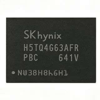
H5TC4G63CFR-H9A - 4Gb DDR3L SDRAM 96-FBGA | SK hynix
部品番号: H5TC4G63CFR-H9A ✓ 生産中| 数量 | 単価 | 小計 |
|---|---|---|
| 1 | $8.5 | $8.50 |
| 10 | $7.8 | $78.00 |
| 100 | $7.2 | $720.00 |
| 500 | $6.8 | $3,400.00 |
| 1,000 | $6.5 | $6,500.00 |
H5TC4G63CFR-H9A 概要
DDR3L SDRAM is a type of synchronous dynamic random-access memory that operates at a lower voltage (1.35V) compared to standard DDR3 (1.5V), reducing power consumption by up to 20% while maintaining backward compatibility with DDR3 environments. It is part of the DDR3 memory family, which uses double data rate architecture to transfer data on both edges of the clock, achieving high bandwidth. DDR3L is widely used in laptops, embedded systems, and networking equipment where energy efficiency is critical.
Key features include fully differential clock inputs (CK, CK), differential data strobe (DQS, DQS), and an on-chip DLL that aligns DQ, DQS, and DQS transitions with CK transitions. The DM (data mask) function masks write data at both rising and falling edges, ensuring data integrity. The device supports burst lengths of 8 and 4 (with burst chop), and features programmable CAS latency and additive latency for flexible timing.
The H5TC4G63CFR-H9A is designed for high-bandwidth, low-power main memory applications. Its 4Gb density and x16 organization make it ideal for applications requiring large memory capacity with a moderate bus width. The 96-ball TFBGA package offers excellent thermal and electrical performance, with a ball pitch of 0.8mm, facilitating high-density PCB layouts.
Typical applications include laptops and ultrabooks, embedded computing, networking switches and routers, and industrial automation systems. The low operating voltage and high bandwidth make it suitable for battery-powered devices and energy-conscious designs.
When designing with this component, ensure proper decoupling capacitors are placed near the VDD and VDDQ pins to minimize noise. The device requires a stable 1.35V supply and careful signal integrity management for the high-speed data bus. Refer to the datasheet for detailed timing parameters and PCB layout guidelines.
ドロップイン代替品: H5TC4G63CFR-H9A — 同一パッケージでピン互換。PCBの作り直しが必要な異なるパッケージの部品は除外されています。
このシリーズのバリエーション
同一シリーズでドロップイン互換のモデル: H5TC4G63CFR-H9A (同一形状・フットプリント) — 相違点: Package, Burst Length, Supply Voltage, CAS Latency, Data Rate.
クイック比較ツール — 並列比較する代替部品を選択:
H5TC4G63AFR-H9A
✅ ドロップイン✓ 在庫あり
$6.5 / 個
データシートを見る →H5TC4G63CFR-H9I
✅ ドロップイン ⚠️ 仕様未検証✓ 在庫あり
$7.2 / 個
データシートを見る →H5TC4G63CFR-H9J
✅ ドロップイン ⚠️ 仕様未検証✓ 在庫あり
$6 / 個
データシートを見る →K4B4G1646E-BYK0
✅ ドロップイン ⚠️ 仕様未検証✓ 在庫あり
$1.8 / 個
データシートを見る →MT41K256M16HA-125
✅ ドロップイン ⚠️ 仕様未検証✓ 在庫あり
$6.3636 / 個
データシートを見る →IS43TR16256AL-125KBL
✅ ドロップイン ⚠️ 仕様未検証✓ 在庫あり
$5.6 / 個
データシートを見る →H5TC4G63CFR-H9A 最大定格&電気的特性
| メモリタイプ | DDR3L SDRAM |
| Memory Density | 4Gb (4294967296 bit) |
| メモリ構成 | 256M x 16 |
| Supply Voltage (VDD) | 1.35V + 0.100 / - 0.067V |
| Supply Voltage (VDDQ) | 1.35V + 0.100 / - 0.067V |
| パッケージ | 96-ball TFBGA |
| Number of Terminals | 96 |
| Package Shape | RECTANGULAR |
| RoHS ステータス | Compliant |
| Lead-Free | Yes |
| ハロゲンフリー | Yes |
| Burst Length | 8, 4 (with burst chop) |
| Differential Clock Inputs | Yes (CK, CK) |
| Differential Data Strobe | Yes (DQS, DQS) |
| On-Chip DLL | Yes |
| DM (Data Mask) | Yes |
H5TC4G63CFR-H9A ピン構成
| ピン A1 | VDD — Power supply |
| ピン A2 | DQ0 — Data input/output 0 |
| ピン A3 | DQ1 — Data input/output 1 |
| ピン A4 | VSS — Ground |
| ピン A5 | DQ2 — Data input/output 2 |
| ピン A6 | DQ3 — Data input/output 3 |
| ピン A7 | VDDQ — Power supply for output |
| ピン A8 | DQ4 — Data input/output 4 |
| ピン A9 | DQ5 — Data input/output 5 |
| ピン A10 | VSS — Ground |
| ピン A11 | DQ6 — Data input/output 6 |
| ピン A12 | DQ7 — Data input/output 7 |
| ピン B1 | VSS — Ground |
| ピン B2 | DQ8 — Data input/output 8 |
| ピン B3 | DQ9 — Data input/output 9 |
| ピン B4 | VDD — Power supply |
| ピン B5 | DQ10 — Data input/output 10 |
| ピン B6 | DQ11 — Data input/output 11 |
| ピン B7 | VSS — Ground |
| ピン B8 | DQ12 — Data input/output 12 |
| ピン B9 | DQ13 — Data input/output 13 |
| ピン B10 | VDDQ — Power supply for output |
| ピン B11 | DQ14 — Data input/output 14 |
| ピン B12 | DQ15 — Data input/output 15 |
| ピン C1 | VDDQ — Power supply for output |
| ピン C2 | VSS — Ground |
| ピン C3 | VDD — Power supply |
| ピン C4 | VSS — Ground |
| ピン C5 | VDDQ — Power supply for output |
| ピン C6 | VSS — Ground |
| ピン C7 | VDD — Power supply |
| ピン C8 | VSS — Ground |
| ピン C9 | VDDQ — Power supply for output |
| ピン C10 | VSS — Ground |
| ピン C11 | VDD — Power supply |
| ピン C12 | VSS — Ground |
| ピン D1 | CK — Clock input |
| ピン D2 | CK — Complementary clock input |
| ピン D3 | VSS — Ground |
| ピン D4 | CKE — Clock enable |
| ピン D5 | VDD — Power supply |
| ピン D6 | VSS — Ground |
| ピン D7 | VDDQ — Power supply for output |
| ピン D8 | VSS — Ground |
| ピン D9 | VDD — Power supply |
| ピン D10 | VSS — Ground |
| ピン D11 | VDDQ — Power supply for output |
| ピン D12 | VSS — Ground |
| ピン E1 | RAS — Row address strobe |
| ピン E2 | CAS — Column address strobe |
| ピン E3 | WE — Write enable |
| ピン E4 | CS — Chip select |
| ピン E5 | VDD — Power supply |
| ピン E6 | VSS — Ground |
| ピン E7 | VDDQ — Power supply for output |
| ピン E8 | VSS — Ground |
| ピン E9 | VDD — Power supply |
| ピン E10 | VSS — Ground |
| ピン E11 | VDDQ — Power supply for output |
| ピン E12 | VSS — Ground |
| ピン F1 | A0 — Address input 0 |
| ピン F2 | A1 — Address input 1 |
| ピン F3 | A2 — Address input 2 |
| ピン F4 | A3 — Address input 3 |
| ピン F5 | VDD — Power supply |
| ピン F6 | VSS — Ground |
| ピン F7 | VDDQ — Power supply for output |
| ピン F8 | VSS — Ground |
| ピン F9 | VDD — Power supply |
| ピン F10 | VSS — Ground |
| ピン F11 | VDDQ — Power supply for output |
| ピン F12 | VSS — Ground |
| ピン G1 | A4 — Address input 4 |
| ピン G2 | A5 — Address input 5 |
| ピン G3 | A6 — Address input 6 |
| ピン G4 | A7 — Address input 7 |
| ピン G5 | VDD — Power supply |
| ピン G6 | VSS — Ground |
| ピン G7 | VDDQ — Power supply for output |
| ピン G8 | VSS — Ground |
| ピン G9 | VDD — Power supply |
| ピン G10 | VSS — Ground |
| ピン G11 | VDDQ — Power supply for output |
| ピン G12 | VSS — Ground |
| ピン H1 | A8 — Address input 8 |
| ピン H2 | A9 — Address input 9 |
| ピン H3 | A10/AP — Address input 10 / Auto-precharge |
| ピン H4 | A11 — Address input 11 |
| ピン H5 | VDD — Power supply |
| ピン H6 | VSS — Ground |
| ピン H7 | VDDQ — Power supply for output |
| ピン H8 | VSS — Ground |
| ピン H9 | VDD — Power supply |
| ピン H10 | VSS — Ground |
| ピン H11 | VDDQ — Power supply for output |
| ピン H12 | VSS — Ground |
| ピン J1 | A12 — Address input 12 |
| ピン J2 | A13 — Address input 13 |
| ピン J3 | BA0 — Bank address 0 |
| ピン J4 | BA1 — Bank address 1 |
| ピン J5 | VDD — Power supply |
| ピン J6 | VSS — Ground |
| ピン J7 | VDDQ — Power supply for output |
| ピン J8 | VSS — Ground |
| ピン J9 | VDD — Power supply |
| ピン J10 | VSS — Ground |
| ピン J11 | VDDQ — Power supply for output |
| ピン J12 | VSS — Ground |
| ピン K1 | BA2 — Bank address 2 |
| ピン K2 | ODT — On-die termination |
| ピン K3 | VSS — Ground |
| ピン K4 | VDD — Power supply |
| ピン K5 | VSS — Ground |
| ピン K6 | VDDQ — Power supply for output |
| ピン K7 | VSS — Ground |
| ピン K8 | VDD — Power supply |
| ピン K9 | VSS — Ground |
| ピン K10 | VDDQ — Power supply for output |
| ピン K11 | VSS — Ground |
| ピン K12 | VDD — Power supply |
| ピン L1 | DM — Data mask |
| ピン L2 | DQS — Data strobe |
| ピン L3 | DQS — Complementary data strobe |
| ピン L4 | VSS — Ground |
| ピン L5 | VDDQ — Power supply for output |
| ピン L6 | VSS — Ground |
| ピン L7 | VDD — Power supply |
| ピン L8 | VSS — Ground |
| ピン L9 | VDDQ — Power supply for output |
| ピン L10 | VSS — Ground |
| ピン L11 | VDD — Power supply |
| ピン L12 | VSS — Ground |
| ピン M1 | VSS — Ground |
| ピン M2 | VDD — Power supply |
| ピン M3 | VSS — Ground |
| ピン M4 | VDDQ — Power supply for output |
| ピン M5 | VSS — Ground |
| ピン M6 | VDD — Power supply |
| ピン M7 | VSS — Ground |
| ピン M8 | VDDQ — Power supply for output |
| ピン M9 | VSS — Ground |
| ピン M10 | VDD — Power supply |
| ピン M11 | VSS — Ground |
| ピン M12 | VDDQ — Power supply for output |
主な用途
H5TC4G63CFR-H9A の用途: 6 件s: Laptops and Ultrabooks, Embedded Computing, Networking Equipment, Industrial Automation, Consumer Electronics, Networking and Communications.
Laptops and Ultrabooks
The H5TC4G63CFR-H9A is ideal for laptops and ultrabooks due to its low 1.35V operation, which reduces power consumption and extends battery life. Its 4Gb density and x16 organization provide sufficient memory capacity for mainstream computing tasks. The 96-ball TFBGA package allows for compact PCB designs, essential for thin and light form factors. With a data rate of up to 1866 Mbps (typical for DDR3L), it delivers the bandwidth needed for smooth multitasking and multimedia applications. The low operating voltage also reduces heat generation, improving thermal management in confined spaces.
おすすめ
Embedded Computing
In embedded systems, the H5TC4G63CFR-H9A provides high-density, low-power memory for applications such as industrial PCs, point-of-sale terminals, and medical devices. Its 1.35V supply reduces power consumption, which is critical for fanless designs. The x16 organization simplifies interfacing with embedded processors that have 16-bit memory buses. The device's support for burst lengths of 8 and 4 allows efficient data transfers, and the on-chip DLL ensures reliable timing. The 96-ball TFBGA package is suitable for automated assembly, and the RoHS compliance meets environmental regulations.
おすすめ
Networking Equipment
The H5TC4G63CFR-H9A is well-suited for networking switches and routers, where high bandwidth and low power are essential. Its 4Gb density allows for large packet buffers, and the x16 organization matches common network processor interfaces. The low 1.35V operation reduces power dissipation in dense line cards, improving system reliability. The differential clock and data strobe inputs ensure signal integrity at high speeds, critical for error-free data transmission. The device's RoHS compliance is important for global market access.
おすすめ
Industrial Automation
In industrial automation, the H5TC4G63CFR-H9A provides reliable memory for PLCs, robotics controllers, and HMI systems. Its wide operating temperature range (if specified) supports harsh environments. The low power consumption reduces heat, which is beneficial in sealed enclosures. The 96-ball TFBGA package offers good thermal performance, and the device's high bandwidth supports real-time data processing. The RoHS compliance ensures environmental safety in industrial settings.
おすすめ
Consumer Electronics
The H5TC4G63CFR-H9A is used in consumer electronics such as smart TVs, set-top boxes, and gaming consoles. Its 4Gb density provides ample memory for multimedia applications, and the low 1.35V operation reduces power consumption, which is important for energy-efficient devices. The x16 organization is compatible with many SoCs, and the compact TFBGA package allows for slim product designs. The device's high bandwidth supports smooth video playback and responsive user interfaces.
おすすめ
Networking and Communications
The H5TC4G63CFR-H9A is also used in communication infrastructure such as base stations and network appliances. Its high density and low power make it suitable for buffer memory in packet processing. The differential signaling ensures reliable operation at high frequencies, and the on-chip DLL helps maintain timing accuracy. The device's RoHS compliance is essential for global deployment. The 96-ball TFBGA package is suitable for high-density PCB designs.
おすすめ
おすすめ製品の概要
エンジニアリング参考データ: H5TC4G63CFR-H9A — 比較、設計ガイダンス、コンプライアンス情報。
選定ガイド
代替品との比較
| パラメータ | この製品 | H5TC4G63AFR-H9A | H5TC4G63CFR-H9I | H5TC4G63CFR-H9J | K4B4G1646E-BYK0 | MT41K256M16HA-125 | IS43TR16256AL-125KBL |
|---|---|---|---|---|---|---|---|
| Package | 96-ball TFBGA | 96-ball TFBGA | 96-ball TFBGA | 96-ball TFBGA | 96-ball FBGA | 96-ball FBGA | 96-ball TFBGA |
| Brand | SK hynix | SK hynix | SK hynix | SK hynix | Samsung | Micron | ISSI |
| Memory Density | 4Gb | 4Gb | 4Gb | 4Gb | 4Gb | 4Gb | 4Gb |
| Organization | 256M x 16 | 256M x 16 | 256M x 16 | 256M x 16 | 256M x 16 | 256M x 16 | 256M x 16 |
| Supply Voltage | 1.35V | 1.35V | 1.35V | 1.35V | 1.35V | 1.35V | 1.35V |
| RoHS Compliant | Yes | Yes | Yes | Yes | Yes | Yes | Yes |
| Speed Grade | H9A (1866 Mbps) | H9A (1866 Mbps) | H9I (1600 Mbps) | H9J (1333 Mbps) | BYK0 (1866 Mbps) | -125 (1600 Mbps) | -125 (1600 Mbps) |
| Data Rate | 1866 Mbps | 1866 Mbps | 1600 Mbps | 1333 Mbps | 1866 Mbps | 1600 Mbps | 1600 Mbps |
主な差別化要因
- Low power consumption (vs K4B4G1646E-BYK0)
- High speed grade (vs MT41K256M16HA-125)
- Same-brand availability (vs IS43TR16256AL-125KBL)
設計ノート
Ensure stable 1.35V supply for VDD and VDDQ. Use low-ESR decoupling capacitors (e.g., 0.1uF and 1uF) placed close to each power pin to minimize noise. The tolerance is +0.100V / -0.067V, so a well-regulated supply is critical. Consider using a dedicated DDR3L power solution to maintain voltage accuracy under load transients.
For high-speed DDR3L signals, maintain controlled impedance (typically 50 ohms single-ended, 100 ohms differential) and keep trace lengths matched within 50 mils. Place the device close to the controller to minimize stub effects. Use ground planes to provide a return path and reduce EMI. Follow the layout guidelines in the SK hynix datasheet for optimal signal integrity.
The H5TC4G63CFR-H9A in a 96-ball TFBGA package has a thermal resistance that depends on PCB design. Ensure adequate thermal vias and copper pour under the package to dissipate heat. The device's low 1.35V operation reduces power dissipation, but in high-density systems, monitor junction temperature to stay within the specified operating range.
コンプライアンス情報
RoHS compliant and lead-free/halogen-free per datasheet. REACH and conflict minerals status not specified in provided data.