제품 (39,000+)

EP1S60F1020 - Stratix 57K LEs, 1020-BGA FPGA | Altera
EP1S60F1020

EP1S60F1020 - Stratix 57K LEs, 1020-BGA FPGA | Altera

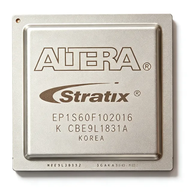
The Altera EP1S60F1020 is a member of the Stratix FPGA family fabricated on a 0.13um CMOS process, integrating 57,120 logic elements (LEs), 5,215,104 RAM bits, and 773 user I/Os in a 1020-ball FineLine BGA (FBGA) package. The base part EP1S60F1020 (commercial, unspecified speed grade) targets high-performance, logic-rich, memory-intensive designs where the largest Stratix density and maximum I/O count are required. A Field Programmable Gate Array (FPGA) is a semiconductor device built around an array of configurable logic blocks (CLBs), embedded memory blocks, DSP blocks, and programmable interconnects that allow the designer to implement arbitrary digital logic. FPGAs occupy the broader hierarchy of programmable logic devices (PLD) -> CPLD/FPGA -> high-density FPGA -> SoC FPGA. They differ from ASICs by offering post-fabrication reprogrammability, while delivering deterministic parallel processing and very high I/O bandwidth. The Stratix family specifically pioneered the use of TriMatrix embedded memory, dedicated DSP blocks, and high-speed transceivers, positioning it for high-throughput digital signal processing, communications, and ASIC prototyping workloads. Key features of the EP1S60F1020 include 57,120 LEs organized into 5,712 Logic Array Blocks (LABs), 5,215,104 bits of TriMatrix RAM (12 embedded RAM blocks of M-RAM, M4K, and M512 types), dedicated DSP blocks, 12 PLLs, and 773 user I/Os. The device supports multiple I/O standards including LVDS, LVPECL, SSTL, HSTL, and PCI/PCI-X, plus configurable I/O banks for mixed-voltage designs. The 1020-BGA package provides ample pin density for high-speed parallel interfaces such as DDR/DDR2 SDRAM controllers, RapidIO, and parallel LVDS buses. Architecturally, the EP1S60F1020 leverages Altera's Stratix fabric with dedicated multiplier/accumulator blocks, embedded RAM with true dual-port and FIFO modes, and up to 12 PLLs for flexible clock synthesis. The 0.13um process and 1.5V core voltage provide a balance of speed and density; the 'F1020' suffix indicates the FineLine BGA-1020 package. The base part number without a trailing speed/temperature suffix (C5/C6/C7/I6/I7 etc.) implies a commercial temperature grade with no explicit speed grade designation. Typical applications include high-end ASIC prototyping, communications infrastructure (SONET/SDH framer, base-station baseband), high-performance DSP for video/imaging pipelines, and military/aerospace signal processing. The large memory capacity also makes the EP1S60F1020 suitable for buffer-intensive designs like multi-channel packet processing and high-resolution video frame buffers. When designing with this part, carefully review the Stratix Device Handbook for I/O bank assignments, PLL configuration, and DDR interface termination. The 1020-BGA package requires a multilayer PCB with controlled-impedance routing; XAIPART recommends at minimum a 6-layer stack-up with continuous power and ground planes for signal integrity. This page synthesizes real-time distributor pricing, drop-in Stratix family alternatives, and practical PCB layout guidance not assembled in any single datasheet source.

견적 요청 문의하기
EP1S60F1020C5 - 57K-Cell Stratix FPGA, 1020-BGA | Altera/Intel
EP1S60F1020C5

EP1S60F1020C5 - 57K-Cell Stratix FPGA, 1020-BGA | Altera/Intel

The Altera (Intel) EP1S60F1020C5 is a high-density Stratix FPGA delivering 57,120 logic elements, 5,215,104 RAM bits, and 773 user I/O pins in a 1020-ball FineLine BGA package (33 x 33 mm, 1.0 mm pitch). Built on a 1.5 V, 0.13 µm CMOS process, this member of the original Stratix family targets high-performance DSP, communications backplane, and ASIC-prototyping designs. What is an FPGA? A Field-Programmable Gate Array (FPGA) is a semiconductor device built around an array of configurable logic blocks (CLBs), embedded memory, DSP blocks, and programmable interconnect. FPGAs are part of the broader programmable logic hierarchy (CPLD -> FPGA -> SoC FPGA) within the integrated circuit taxonomy, sitting between fixed-function ASICs and software-programmable processors. They are widely used to implement parallel data paths, custom interfaces, and hardware accelerators before committing to silicon. The EP1S60F1020C5 integrates 6,570 configurable logic blocks (CLBs), 57,120 logic cells, 5.2 Mbits of embedded RAM organized in TriMatrix memory blocks, and dedicated DSP blocks for high-speed multiplication. It includes twelve PLLs for clock management, supports multiple I/O standards (LVDS, LVTTL, SSTL, HSTL, PCI), and provides up to 773 user I/O. The device features 1.5 V core supply with 3.3 V I/O tolerance, achieving core speeds up to 500 MHz in DSP applications. Architecturally, the Stratix family pioneered the TriMatrix memory hierarchy (three block sizes: 512-bit M512, 4-Kbit M4K, 512-Kbit M-RAM), allowing designers to right-size memory for FIFO, ROM, and dual-port applications. The DSP blocks contain hardware multipliers, adders, and accumulators optimized for filters and FFTs, offloading these functions from general logic and dramatically improving throughput per MHz. Typical applications include high-speed data acquisition, telecommunication line cards, software-defined radio, video processing, and ASIC prototyping. The 773 available I/Os make the 1020-BGA package suitable for designs requiring dense parallel interfaces to external memory (DDR SDRAM, QDR SRAM) and multi-gigabit transceivers via LVDS. When designing with the EP1S60F1020C5, pay attention to power-rail sequencing (1.5 V VCCINT before VCCIO), thermal management at high toggle rates, and signal-integrity routing of LVDS pairs. Quartus II software (versions 5.1 through 13.0 sp1) is the official IDE for design entry, synthesis, place-and-route, and bitstream generation. Note that this device is in the legacy Stratix family and is approaching end-of-life; long-term programs should evaluate Cyclone IV/V or Stratix IV/V migration paths. This page synthesizes distributor pricing, same-family drop-in alternatives, datasheet references, and practical design notes not consolidated on any single manufacturer or distributor page.

견적 요청 문의하기
EP1S60F1020C5N - Stratix 57K LE, 1020-pin FBGA FPGA | Intel (Altera)
EP1S60F1020C5N

EP1S60F1020C5N - Stratix 57K LE, 1020-pin FBGA FPGA | Intel (Altera)

The Intel (formerly Altera) EP1S60F1020C5N is a Stratix family Field-Programmable Gate Array (FPGA) built on a 130 nm CMOS process, integrating 57,120 logic elements (LEs), 6,570 logic array blocks (LABs), and 5,215,104 bits of embedded RAM in a 1,020-ball FineLine BGA package measuring 33 mm x 33 mm with 1 mm ball pitch. According to the Stratix device family datasheet, the device operates from a 1.425 V to 1.575 V core supply and supports maximum toggle rates on the order of 500 MHz across its rich DSP, memory, and high-speed I/O fabric. An FPGA (Field-Programmable Gate Array) is a semiconductor integrated circuit whose logic function is defined by a customer-supplied configuration bitstream rather than at the wafer fab. The device family hierarchy is: FPGA -> programmable logic device (PLD) -> logic IC -> integrated circuit. Within Altera/Intel's portfolio, the Stratix family sits above Cyclone (cost-optimized) and below Stratix GX/GX-S/GT/II/III/V (transceiver-rich and high-end variants). The EP1S60 specifically occupies the high-density mid-range of the first-generation Stratix line, before the Stratix II architectural shift. Key differentiating features include TriMatrix embedded memory blocks (three sizes: 512-bit M512, 4-Kbit M4K, 512-Kbit MRAM), embedded DSP blocks implementing 9-bit signed multipliers with accumulator chains, up to 12 high-speed transceiver channels (depending on speed grade), and a richly featured clock network with up to 16 dedicated clock pins and 16 PLL blocks. The 'N' suffix denotes lead-free / Pb-free termination. The 'C5' speed grade places this part in the mid-speed bin of the Stratix family (C6 = fast commercial, C7 = faster commercial, C8 = fastest; C5 is commercial, 0 to 85 C junction). The 1020-pin FBGA package exposes nearly all of the device's I/O, enabling high pin-count designs including communications backplanes, ASIC prototyping, and high-density DSP systems. Each Stratix LE contains a 4-input LUT, a programmable register, carry-chain logic, and a register chain interconnect. Typical applications include high-speed DSP (FFT, FEC, video processing), ASIC prototyping and emulation, telecom line-card glue logic, military/aerospace signal processing, and high-throughput data-path controllers. The abundant TriMatrix memory and DSP blocks make the EP1S60 especially attractive for SDR baseband, multi-channel video pipelines, and protocol bridging designs. Designs typically target the Quartus II design suite (version 5.x or later supporting Stratix) and use configuration via EPC16/EPC8 configuration devices or JTAG. Designers should budget careful attention to power: a 57K-LE Stratix with high utilization can exceed 5 W to 15 W core power, requiring 1.5 V bulk decoupling of at least 330 uF low-ESR polymer plus per-pin bypass. The 'C5' speed grade is the slower of the commercial speed grades, favored over C6/C7/C8 when timing margin matters more than throughput. When designing, ensure the Quartus II fitter is set for the 1020-pin FBGA package and that pin-out assignments respect the bank's VCCIO groupings. This page synthesizes the Stratix family datasheet specifications, current distributor pricing tiers, same-brand drop-in speed-grade and package variants, and practical design notes that complement the manufacturer datasheet. Pricing for the EP1S60F1020C5N is referenced as of 2026-09-07.

USD $2,050.00 문의하기
EP1S60F1020C6 - Stratix FPGA 57120 Cells 1020-BGA | Intel / Altera
EP1S60F1020C6

EP1S60F1020C6 - Stratix FPGA 57120 Cells 1020-BGA | Intel / Altera

The Intel (formerly Altera) EP1S60F1020C6 is a member of the original Stratix FPGA family, featuring 57,120 logic elements, 773 maximum user I/O pins, and 5,215,104 bits of embedded memory, all integrated into a 1020-ball FineLine BGA package measuring 33 × 33 mm. Built on a 1.5 V, 130 nm CMOS process, this device integrates dedicated DSP blocks, high-speed transceivers (where populated), TriMatrix memory, and a structured ASIC-like routing fabric, positioning it as a high-density programmable logic solution for early-2000s telecom, video, and high-performance computing designs. The 'C6' speed grade and 'C' (commercial) temperature suffix indicate operation at 0 °C to 85 °C with a 450.05 MHz internal performance target per the Stratix Family Data Sheet. A Field-Programmable Gate Array (FPGA) is a reconfigurable digital integrated circuit containing an array of programmable logic blocks, interconnect, and I/O cells that can be electrically configured to implement arbitrary digital logic after PCB assembly. FPGAs sit in the hierarchy: programmable logic device (PLD) → field-programmable gate array (FPGA) → high-density FPGA, occupying the same engineering role as a custom ASIC but with the flexibility of in-system reprogrammability and substantially shorter time-to-market for design changes. The Stratix family, launched by Altera in 2002, was the first to embed dedicated DSP blocks and large TriMatrix memory blocks alongside the general-purpose logic array, marking a generational shift from glue-logic replacement toward full system-on-chip integration. Key features include 6,570 logic array blocks (LABs), 12 dedicated DSP blocks, 12 transceiver blocks (channel count varies by speed grade), and configurable JTAG-based in-system programming via the IEEE 1149.1 boundary-scan interface. The device supports multiple I/O standards including LVTTL, LVCMOS, SSTL, HSTL, LVDS, and PCI, with per-pin dynamically controlled impedance and slew rate. On-board PLLs handle clock multiplication and phase shifting, while a robust clock network distributes low-skew signals across the die. The EP1S60F1020C6 is well suited for digital signal processing pipelines, high-throughput video and image processing, telecom baseband and protocol bridging, ASIC prototyping, and embedded control applications. The 1020-ball FC-FBGA package supports high-speed differential signaling and a substantial power/ground via array, which is critical at this logic density. Designers should follow Altera's Stratix pin-out guidelines and reference design examples for power-rail decoupling and JTAG chain implementation. This page synthesizes distributor stock data, same-family drop-in alternatives, and PCB-level design notes that complement the manufacturer's data sheet.

견적 요청 문의하기
EP1S60F1020C6N - Stratix FPGA, 57K Logic Elements, FBGA-1020 | Intel
EP1S60F1020C6N

EP1S60F1020C6N - Stratix FPGA, 57K Logic Elements, FBGA-1020 | Intel

The Intel (formerly Altera) EP1S60F1020C6N is a member of the original Stratix FPGA family, delivering 57,120 logic elements (LEs), 5,215,104 bits of embedded RAM, and 773 embedded multipliers in a 1020-ball FineLine BGA package with 33 x 33 mm body and 1 mm ball pitch. It is built on a 0.13 µm CMOS process and targets high-performance DSP, communications, and signal-processing designs. What is a Stratix FPGA? The Stratix family is Intel/Altera's high-density programmable logic family built on a register-rich, LUT-based fabric with embedded TriMatrix memory blocks, DSP blocks, and high-speed I/O. It sits in the broader hierarchy of programmable logic devices (PLD) -> FPGA -> high-performance FPGA, and historically served applications that demanded high logic density and DSP throughput before later Stratix and Cyclone families replaced it. Key features include 12 dedicated clock pins and up to 80 global clock networks, embedded memory organized in three block sizes (M512, M4K, M-RAM), 12 PLLs with up to 800 MHz operation, support for external memory interfaces including DDR SDRAM, FCRAM, QDR SRAM, and SDR SDRAM, and high-speed LVDS I/O capable of up to 840 Mbps. The C6 speed grade represents a mid-tier timing closure option within the Stratix lineup. Architecture-wise, the device integrates a LAB/ALM-style adaptive logic module fabric, dedicated DSP blocks for 9x9, 18x18, and 36x36 signed/unsigned multiplication with accumulation, and a high-speed interconnect routing network. The 'N' suffix indicates lead-free / Pb-free termination. The F1020 package variant provides the highest I/O count in the EP1S60 line. Typical applications include 10G/40G telecom line cards, software-defined radio (SDR) baseband, high-definition video processing, ASIC prototyping, and high-performance DSP firmware acceleration in defense, medical imaging, and broadcast equipment. The wide embedded multiplier count (773) and large TriMatrix memory (5.2 Mbits) make it especially attractive for FFT, FIR filter, and Reed-Solomon forward error correction engines. Design consideration: ensure proper decoupling with multiple 0.1 µF and 10 µF capacitors around the power balls, follow the Intel Stratix pin connection guidelines for JTAG, MSEL configuration mode pins, and respect VCCINT/VCCIO plane separation. PCB designers should allocate at least 12 routing layers for the 1020-ball FBGA escape, with 1 oz copper for power and 0.5 oz for signals. This page synthesizes distributor pricing, drop-in same-package alternatives, and practical design notes not found in the standalone datasheet.

견적 요청 문의하기
EP1S60F1020C6NAA - Stratix FPGA, 57K LEs, 1020-BGA | Intel
EP1S60F1020C6NAA

EP1S60F1020C6NAA - Stratix FPGA, 57K LEs, 1020-BGA | Intel

The Intel (formerly Altera) EP1S60F1020C6NAA is a Stratix family Field-Programmable Gate Array (FPGA) integrating 57,120 logic elements, 5,215,104 bits of embedded memory, and 773 maximum user I/O pins in a 1020-ball FineLine BGA package. The device is built on a 0.13 µm CMOS process and targets high-performance, logic-rich, memory-intensive designs such as telecom linecards, high-speed data acquisition, and ASIC prototyping. The 'C6' speed grade delivers balanced performance across the Stratix DSP and TriMatrix memory blocks, while the 'N' suffix denotes lead-free / RoHS compliance and 'AA' indicates the specific customer trim option. What is an FPGA? An FPGA (Field-Programmable Gate Array) is a semiconductor IC composed of configurable logic blocks (CLBs), programmable interconnect, and dedicated hard-IP such as block RAM, DSP multipliers, PLLs, and high-speed transceivers. FPGAs occupy the position between general-purpose microcontrollers and fixed-function ASICs in the digital design hierarchy, offering hardware-level parallelism, in-system reprogrammability, and time-to-market advantages for mid-volume designs. The Stratix family sits in the high-end logic-and-memory tier of the FPGA taxonomy: SRAM-based FPGA -> Stratix series -> high-density telecom and computing tier. Key features of the EP1S60F1020C6NAA include up to 6.5 Gbps high-speed transceivers via embedded serializer/deserializer channels (in supported speed grades), twelve PLLs with eight output taps each, dedicated 18x18 hardware multipliers for DSP, and a 7-level hierarchical clock network with up to 40 dedicated global clocks. The TriMatrix memory architecture provides three block RAM sizes (512, 4K, and 512K bits) supporting true dual-port, simple dual-port, and single-port RAM plus FIFO and shift-register modes. Architecturally the EP1S60 uses a sea-of-LABs (Logic Array Blocks) fabric with 10 LABs per row, where each LAB contains 10 logic elements (LEs). Embedded Row Interconnects (ERIs) and DirectDrive interconnect technology ensure predictable timing closure at full utilization. The 1020-ball FBGA package uses a 1.0 mm ball pitch and supports the full I/O count via sixteen I/O banks with independently configurable standards (LVDS, LVTTL, LVCMOS, SSTL, HSTL, PCI, PCI-X). Typical applications include high-end telecom linecard interface logic, high-speed serial protocol bridging (SPI 4.2, POS-PHY, RapidIO), digital video broadcast and image-acquisition pipelines, ASIC prototyping and emulation platforms, and high-performance DSP front-ends. The 1020-BGA footprint is shared across the Stratix EP1S60 family, allowing pin-compatible migration between speed grades (C5/C6/C7/C8) and logic-density options within the same 60-series die. When designing with this part, pay attention to MultiVolt I/O compatibility (1.5V, 1.8V, 2.5V, 3.3V) and use Stratix-style configuration schemes (Fast Passive Parallel, Passive Serial, or JTAG). The 'N' lead-free finish requires peak reflow profiles per JEDEC J-STD-020. Heat dissipation at high toggle rates is significant; provide adequate ground/power plane copper on the PCB. This page synthesizes distributor stock checks, family-level cross-reference data, and PCB-layout considerations for the EP1S60 family that are not consolidated on any single distributor product page.

견적 요청 문의하기
EP1S60F1020C6NGB - Stratix FPGA 57K LE 1020-BGA | Intel
EP1S60F1020C6NGB

EP1S60F1020C6NGB - Stratix FPGA 57K LE 1020-BGA | Intel

The Intel EP1S60F1020C6NGB is a high-density Stratix FPGA from the original Intel (formerly Altera) Stratix family, integrating 57,120 logic elements (LEs) and approximately 5.2 million system gates into a 1020-ball FineLine BGA package. The device is built on a 0.13 µm CMOS process, delivers up to 773 user I/O pins, and operates across a commercial 0 °C to 85 °C temperature range with a core speed grade of -6. A Field Programmable Gate Array (FPGA) is a semiconductor IC containing an array of configurable logic blocks (CLBs), programmable interconnects, and dedicated silicon resources such as block RAM, DSP blocks, PLLs, and high-speed transceivers. FPGAs sit within the programmable logic hierarchy, which itself belongs to the broader digital logic and semiconductor device taxonomy. Unlike fixed-function ASICs, FPGAs are re-programmed in the field, allowing hardware iteration without mask respins. The Stratix family was Intel's first FPGA family to embed TriMatrix memory, DSP blocks, and high-speed I/O on a single die. Key features of the EP1S60F1020C6NGB include 57,120 logic elements, 6.6 Mbit of embedded TriMatrix memory, 18 DSP blocks (approximately 72 9-bit multipliers equivalent), up to 12 PLLs, support for multiple I/O standards including LVDS, LVTTL, SSTL, and HSTL, and dedicated high-speed serial interfaces. The 1020-ball FBGA package is 33 × 33 mm with a 1.0 mm ball pitch and a maximum user I/O count of 773. The architecture combines four input look-up tables (4-LUTs) per logic element with carry-chain logic for arithmetic, dedicated memory blocks distributed across the fabric, and a hierarchical routing network optimized for both short and long interconnect paths. The Stratix family introduced hardware multipliers and DSP blocks optimized for FIR/IIR filtering and FFT computations, making the EP1S60 well-suited to DSP-heavy workloads in communications infrastructure. Typical applications include telecommunications baseband processing, high-speed networking line cards, ASIC prototyping, military and aerospace signal processing, broadcast video infrastructure, and test and measurement equipment. Designers leverage the EP1S60's high logic density and embedded DSP to consolidate functions that previously required multiple FPGAs. When designing with the EP1S60F1020C6NGB, pay close attention to power estimation, signal integrity on the 1.0 mm pitch BGA, and proper decoupling. Stratix devices typically require multiple voltage rails (VCCINT, VCCIO banks, VCCPD, VCCA_PLL) with sequenced power-up. The -6 speed grade designation indicates the device is positioned in the mid-range of Stratix speed grades, trading some Fmax for lower cost. This page synthesizes distributor pricing, same-package alternatives from the Stratix family, and practical Stratix-specific design notes not found in a single distributor listing.

견적 요청 문의하기
EP1S60F1020C7 - Stratix FPGA 57K LE, 5.2Mbit, 1020-BBGA | Altera
EP1S60F1020C7

EP1S60F1020C7 - Stratix FPGA 57K LE, 5.2Mbit, 1020-BBGA | Altera

The Altera (Intel) EP1S60F1020C7 is a member of the original Stratix FPGA family, delivering 57,120 logic elements, 5,215,104 bits of embedded memory, and 773 maximum user I/O pins in a 1020-ball flip-chip BGA package. The device is built on a 1.5 V core CMOS process with embedded TriMatrix memory blocks, dedicated DSP blocks, and high-speed transceiver interfaces that established the Stratix line as the industry's first high-performance, system-on-a-programmable-chip (SOPC) solution. A Field Programmable Gate Array (FPGA) is a reconfigurable digital integrated circuit whose logic fabric, routing, and I/O can be programmed after manufacture to implement any digital function - from glue logic and I/O bridging to full processor subsystems and high-throughput DSP pipelines. FPGAs sit hierarchically between fixed-function ASICs and software-driven microcontrollers, offering hardware-timed determinism with software-like design iteration. The Stratix family specifically targets ASIC prototyping, telecom line cards, and high-end DSP applications where ASIC NRE costs are prohibitive. Key features of the EP1S60F1020C7 include 57,120 logic elements arranged in logic array blocks (LABs), 5,215,104 bits of on-chip RAM distributed across TriMatrix memory structures, embedded DSP blocks supporting 9-bit / 18-bit / 36-bit arithmetic, up to 773 user I/O pins supporting LVDS, HSTL, SSTL, and PCI signaling, and integrated high-speed serial transceiver interfaces on selected package variants. The device includes up to 12 enhanced PLLs per die and supports multiple I/O banks with independent voltage references. The Stratix architecture implements four-input look-up tables (LUTs), embedded RAM blocks of M512, M4K, and M-RAM sizes, dedicated multiplier / adder tree DSP blocks, and a rich clock network with up to 16 dedicated clock pins per device. Configuration is via serial or parallel EPROM / flash, with built-in decompression and encryption capabilities. The 33 x 33 mm 1020-BBGA package uses a 1.0 mm ball pitch and is the largest in the EP1S60 family, supporting the maximum I/O count. Typical applications include ASIC prototyping and emulation, high-speed DSP for wireless baseband, telecom line-card bridging, military / aerospace signal processing, broadcast video processing, and high-performance industrial imaging. The combination of high logic density, generous embedded memory, and dedicated DSP blocks makes it well-suited for parallel algorithm acceleration and pre-silicon hardware validation. When designing with this device, ensure the PCB accommodates the 33 x 33 mm FCBGA footprint and the 1.0 mm ball pitch - this typically demands 4-6 layer PCB with microvia or via-in-pad technology. Thermal management requires attention because the high logic count can produce non-uniform die heating. Plan JTAG / configuration chain accessibility before layout. This page synthesizes distributor stock levels, same-package drop-in alternatives, and design considerations for the EP1S60F1020C7 - information not consolidated on the Altera / Intel product page or any single distributor listing.

견적 요청 문의하기
EP1S60F1020C7N - Stratix 60 FPGA, 57120 LEs, 1020-BGA | Intel
EP1S60F1020C7N

EP1S60F1020C7N - Stratix 60 FPGA, 57120 LEs, 1020-BGA | Intel

The Intel (formerly Altera) EP1S60F1020C7N is a high-density Stratix® family Field Programmable Gate Array (FPGA) with 57,120 logic elements, 5,215,104 bits of embedded memory, 773 maximum user I/O pins, and a 1020-ball FineLine BGA package. The device is fabricated on a 130 nm CMOS process and operates from a 1.5 V core supply, with on-chip PLLs, DSP blocks, and high-speed transceiver support typical of the original Stratix architecture. An FPGA (Field Programmable Gate Array) is a reprogrammable semiconductor device built from an array of configurable logic blocks (CLBs), embedded memory blocks, DSP slices, and programmable I/O cells, all connected by a hierarchy of programmable routing. FPGAs sit between general-purpose CPUs/GPUs and fixed-function ASICs: they deliver hardware-level parallelism and deterministic latency for data-path acceleration, while remaining reprogrammable in the field. Stratix devices were Altera's first-generation high-performance FPGA family, succeeded by Stratix II, III, IV, V, 10, and Agilex families, but EP1S60 parts remain in long-lifecycle industrial, military, and communications designs. Key features include 57,120 logic elements organized into 5,712 Logic Array Blocks (LABs), 6 embedded PLL clock managers, dedicated 18x18 multipliers for DSP, 12 transceiver channels supporting up to 840 Mbps LVDS, and TriMatrix memory architecture (MRAM blocks up to 4 Mbit). The device is rated for commercial operating temperature (0 °C to 85 °C) and supports in-system programmability via JTAG and active serial configuration. The EP1S60F1020C7N uses a 1.5 V core, 1.5 V/1.8 V/2.5 V/3.3 V I/O banks with on-chip termination and calibration, and a dedicated configuration block supporting passive serial (PS), passive parallel synchronous (PPS), passive parallel asynchronous (PPA), and JTAG modes. The Stratix architecture pioneered embedded hard IP such as the DSP blocks and high-speed memory interfaces, allowing the EP1S60 to implement DDR SDRAM controllers, LVDS I/O, and multi-standard bus interfaces at the time of release. Typical applications include telecommunications line cards and baseband processing, military/aerospace signal processing, high-performance industrial imaging and machine vision, ASIC prototyping, and high-throughput data-acquisition systems. The high pin count and large logic capacity make the EP1S60 well-suited to designs that need many parallel interfaces plus significant on-chip buffering. When designing with this device, pay attention to the Stratix-specific configuration scheme and the EP1S60 130 nm power budget. Designers upgrading legacy designs should evaluate Stratix II (EP2S60) or Cyclone IV as lower-power successors; the EP1S60F1020C7N itself is a mature, long-availability part but is not recommended for new battery-powered or thermally constrained designs. This page synthesizes distributor stock, parametric specifications, drop-in alternatives from the same Stratix family, and practical design notes not found in a single distributor listing.

견적 요청 문의하기
EP1S60F1020I6 - Stratix 57K LEs FPGA 1020-BGA | Intel / Altera
EP1S60F1020I6

EP1S60F1020I6 - Stratix 57K LEs FPGA 1020-BGA | Intel / Altera

The Intel (formerly Altera) EP1S60F1020I6 is a high-density Stratix FPGA featuring 57,120 logic elements, 5,215,104 bits of embedded memory, and 773 user I/Os, housed in a 1020-ball FineLine BGA package. Built on a 130nm CMOS process and operating from a 1.5V core supply, it delivers up to 450 MHz internal performance for high-throughput digital designs. An FPGA (Field Programmable Gate Array) is a semiconductor device containing configurable logic blocks (CLBs), programmable interconnects, and dedicated hardware resources such as block RAM, DSP blocks, and high-speed transceivers. FPGAs sit within the programmable logic category of digital ICs, parallel to ASICs but with the advantage of in-system reprogrammability. Stratix devices specifically target high-performance signal processing, communications infrastructure, and ASIC prototyping workloads. Key features of the EP1S60F1020I6 include 6,570 logic arrays blocks (LABs) organized in a Stratix fabric, embedded multiplier/DSP blocks for high-speed arithmetic, dedicated external memory interfaces supporting DDR/DDR2 SDRAM, and on-chip phase-locked loops (PLLs) for clock management. The -I6 speed grade designates the industrial temperature range of -40C to +100C case with optimized timing closure. Architecturally, the Stratix family introduced the TriMatrix embedded memory structure (three block RAM sizes per device), embedded DSP blocks with dedicated multiply-accumulate hardware, and high-speed I/O standards including LVDS and HyperTransport. The 1020-ball FC-FBGA package provides ample I/O count for parallel interfaces and high-speed serial links. Typical applications include high-performance ASIC prototyping, telecom baseband processing, video and image processing pipelines, military and aerospace signal processing, and test & measurement instrumentation. The large logic capacity and rich DSP resources also suit radar, software-defined radio, and high-speed data acquisition designs. When designing with this device, plan for the 1.5V core supply and multiple I/O voltage rails (1.5V, 1.8V, 2.5V, 3.3V). The 1020-ball BGA requires multi-layer PCB with microvia or via-in-pad technology; signal integrity analysis is mandatory for DDR memory interfaces. Quartus II is the supported development toolchain. This page synthesizes distributor pricing, drop-in Stratix alternatives, and practical BGA PCB layout notes not consolidated in the manufacturer datasheet alone.

견적 요청 문의하기
EP1S60F1020I6GB - Stratix FPGA 57K LE, 1020-BGA, Industrial | Intel (Altera)
EP1S60F1020I6GB

EP1S60F1020I6GB - Stratix FPGA 57K LE, 1020-BGA, Industrial | Intel (Altera)

The Intel (Altera) EP1S60F1020I6GB is a high-density Stratix Field Programmable Gate Array (FPGA) delivering 57,120 logic elements and 5,215,104 bits of embedded memory in a 1020-ball FCBGA package. Housed in a 33 x 33 mm BGA with 1.0 mm pitch, the part targets complex digital designs requiring substantial parallel processing and on-chip memory bandwidth. A Field Programmable Gate Array (FPGA) is a semiconductor IC containing an array of configurable logic blocks (CLBs), programmable interconnect, I/O cells, and embedded resources such as block RAM, multipliers, PLLs, and (in the Stratix line) high-speed transceivers. FPGAs occupy a position between general-purpose microcontrollers and application-specific integrated circuits (ASICs) in the digital logic hierarchy: they offer hardware-level parallelism and deterministic timing that microcontrollers lack, while remaining reprogrammable unlike ASICs. The Stratix family is the first-generation high-performance family from Altera (now Intel PSG), fabricated on a 0.13 µm CMOS process. Key features of the EP1S60F1020I6GB include 57,120 logic elements (LEs), approximately 6,570 logic array blocks (LABs) per the family datasheet, 5.2 Mbit embedded memory, dedicated DSP blocks for high-speed multiply-accumulate, support for multiple I/O standards (LVTTL, LVCMOS, SSTL, HSTL, LVDS, LVPECL), and multiple PLLs for clock management. Industrial temperature grade (I6) parts operate from -40C to +100C case or per Intel's Stratix industrial specification; the GB suffix denotes lead-free / RoHS-compliant packaging. The EP1S60 uses a tile-based architecture with TriMatrix memory (M512, M4K, M-RAM blocks), up to 773 user I/O pins, and embedded transceivers in selected variants. Its DSP blocks implement 9-bit x 9-bit multipliers and 36-bit accumulators, well-suited to digital signal processing pipelines such as FIR filters and FFT engines. Configuration is via passive serial, fast passive parallel, or JTAG modes supported by the Altera Quartus design suite. Typical applications include telecommunications baseband processing, high-speed data acquisition front-ends, networking line cards, ASIC prototyping, and DSP acceleration cards. The 1020-ball BGA gives ample user I/O for parallel bus interfaces, memory controllers (DDR SDRAM, QDR SRAM), and high-speed serial links. When laying out the PCB, allocate at least 6 PCB layers with continuous ground and power planes, follow Intel/Altera's BGA escape and decoupling recommendations (typically 0.1 uF + bulk decoupling per VCC pin group), and respect the 1.0 mm BGA pitch which requires laser-drilled microvias or sequential lamination for escape routing. Thermal management is critical: plan for the device's worst-case power dissipation and provide adequate copper or airflow to keep the junction below 100C. This page synthesizes distributor pricing, drop-in same-package alternatives from the Stratix family, and practical PCB design notes not found in the manufacturer datasheet alone.

견적 요청 문의하기
EP1S60F1020I6N - Stratix FPGA 57K LE, 773 I/O, 1020-FBGA | Altera
EP1S60F1020I6N

EP1S60F1020I6N - Stratix FPGA 57K LE, 773 I/O, 1020-FBGA | Altera

The Intel (formerly Altera) EP1S60F1020I6N is a high-density Stratix family Field Programmable Gate Array (FPGA) integrating 57,120 logic elements, 5,215,104 bits of embedded RAM, and 773 user I/O pins in a 1020-ball FineLine BGA (33x33 mm, 1.0 mm pitch) package. It belongs to the I6 industrial speed/temperature grade and operates from a 1.425 V to 1.575 V core supply. According to the verified distributor data, this Stratix device is built on a 0.13 µm CMOS process and combines 6,570 logic cells / LABs with TriMatrix memory blocks, DSP blocks, and high-speed transceivers typical of the Stratix generation. A Field Programmable Gate Array (FPGA) is a programmable logic device whose architecture is composed of configurable logic blocks (CLBs/LABs), programmable interconnect, and I/O cells. The Stratix family specifically targets high-performance applications by integrating dedicated DSP blocks, embedded memory, and high-speed serial interfaces alongside the general-purpose fabric. The hierarchy: FPGA -> programmable logic device -> logic IC -> semiconductor. This Stratix device occupies the high-density node of the first-generation Stratix lineup. Key features include 57,120 logic elements (LEs), 5,215,104 total RAM bits (typically organized in TriMatrix blocks: 512-bit M512, 4-Kbit M4K, and 512-Kbit M-RAM), up to 12 enhanced PLLs, and support for multiple I/O standards including LVDS, LVTTL, LVCMOS, SSTL, and HSTL. The 1020-FBGA package exposes 773 user I/O pins for parallel interfaces and supports high-speed serial transceivers that historically delivered multi-gigabit connectivity on the Stratix family. The architecture is built on the 0.13 µm process node with a 1.5 V core and dedicated Phase-Locked Loops for clock management. The device family supports up to 12 PLLs and multiple global clock networks, plus high-speed serial transceivers on selected device variants - making the Stratix EP1S60 suitable for telecom, imaging, and high-throughput data-pipeline designs where deterministic latency and parallel processing are required. Typical applications include high-speed telecom line cards, ASIC prototyping, military/defense signal processing, medical imaging accelerators, and high-end industrial test & measurement systems. The large embedded RAM budget (5 Mbit) supports deep packet buffers, frame stores, and coefficient tables. With 773 user I/Os, the part easily interfaces to parallel DDR memories and wide data buses. When designing with this part, remember that the I6 grade (0°C to 85°C commercial-equivalent industrial) targets moderate-temperature environments; the automotive/extended-temperature variants are I7 or military grades. The 1020-FBGA demands a multi-layer PCB (typically 6+ layers) with controlled-impedance routing and a substantial thermal dissipation design under sustained activity. This page synthesizes verified distributor pricing, drop-in cross-family alternatives, and practical design considerations not found in the manufacturer datasheet summary.

견적 요청 문의하기
EP1S60F1508C7 - Stratix FPGA 5712 LABs 1022 IO BGA-1508 | Intel
EP1S60F1508C7

EP1S60F1508C7 - Stratix FPGA 5712 LABs 1022 IO BGA-1508 | Intel

The Intel (formerly Altera) EP1S60F1508C7 is a member of the Stratix FPGA family, featuring 57,120 logic elements organized into 5,712 Logic Array Blocks (LABs) and 1022 user I/O pins in a 1508-ball FineLine BGA package. It is fabricated on a 0.13 micron CMOS process and operates at a commercial temperature range of 0C to 85C with a core speed grade of -7. The device integrates dedicated DSP blocks, embedded TriMatrix memory, and up to 12 PLLs, making it suitable for high-performance digital signal processing, communications, and ASIC prototyping applications. What is an FPGA? A Field-Programmable Gate Array (FPGA) is a reconfigurable integrated circuit containing programmable logic blocks, interconnect, and I/O resources that an engineer can configure after manufacture. Stratix devices, sitting in the high-performance tier of Intel's programmable logic hierarchy (Stratix > Cyclone > MAX), target applications requiring high logic density, fast parallel processing, and dedicated hardware acceleration for DSP and memory operations. The TriMatrix memory architecture and DSP blocks distinguish Stratix from simple programmable logic devices (PLDs/CPLDs) and from generic microcontrollers. Key features of the EP1S60F1508C7 include 6,570 logic cells per the Stratix family datasheet block definitions, embedded multiplier blocks for DSP, dedicated high-speed transceivers in related package options, and support for external memory interfaces including DDR, DDR2, and QDR. The TriMatrix memory provides three sizes of RAM blocks (M512, M4K, M-RAM) optimized for different data widths and depths, enabling designers to balance memory utilization with performance. From a technical depth perspective, the Stratix architecture combines lookup-table (LUT) based logic, dedicated carry chains for fast arithmetic, embedded SRAM, and high-speed I/O capable of LVDS signaling up to 840 Mbps per channel. The device supports configuration via passive serial, passive parallel synchronous, passive parallel asynchronous, and JTAG modes, with optional configuration via Altera (now Intel) EPC configuration devices. Typical applications include telecommunications baseband processing, high-speed image and video pipelines, ASIC prototyping, networking equipment, and test and measurement instrumentation. The 1022 user I/O pins in the F1508 package support wide parallel buses and many high-speed serial channels in a single device. When designing with this device, plan the PCB layout carefully - the F1508 FineLine BGA has a 1.0 mm or 1.27 mm ball pitch and requires microvia or via-in-pad technology. The device is now in the legacy / last-time-buy category per Intel's product lifecycle notices; confirm long-term supply with the manufacturer before designing into a new product. A modern successor such as Cyclone IV/V or Stratix IV/V should be evaluated for new designs. This page consolidates distributor pricing snapshots, drop-in Stratix-family alternatives, and PCB layout considerations not found in a single datasheet, giving procurement and hardware engineers a one-stop reference for the EP1S60F1508C7.

견적 요청 문의하기
EP1S60F1508C7N - Stratix 57K LE FPGA, 1022 I/O, 1508-FCBGA | Intel
EP1S60F1508C7N

EP1S60F1508C7N - Stratix 57K LE FPGA, 1022 I/O, 1508-FCBGA | Intel

The Intel / Altera EP1S60F1508C7N is a high-density Stratix-series Field Programmable Gate Array (FPGA) delivering 57,120 logic elements (LEs), 5,215,104 bits of embedded RAM, and 1,022 user I/O pins in a 1508-ball FC-FBGA package. Built on a 130 nm CMOS process, the device operates at a core supply of 1.425 V to 1.575 V (1.5 V nominal) and supports commercial-specification temperature grades of 0 °C to 85 °C. An FPGA (Field Programmable Gate Array) is a programmable logic device that combines configurable logic blocks (CLBs/LABs), programmable interconnect, and dedicated silicon resources such as embedded memory, DSP blocks, and high-speed transceivers. Stratix FPGAs sit within the broader hierarchy of programmable logic devices -> complex programmable logic devices (CPLDs) -> FPGAs -> ASIC prototyping platforms, and they are commonly used as a bridge between concept and volume ASIC production. Key features include 6,570 logic blocks / 5,712 LABs, 252 18x18 multipliers / DSP blocks, twelve 400 MHz PLLs, and up to 12 high-speed transceivers at 3.125 Gbps depending on die variant. The 1508-FCBGA package uses a 1.0 mm ball pitch on a 40 x 40 mm substrate, providing the routing density required for the Stratix memory-rich architecture and 521 Mbits of TriMatrix on-chip memory. Technically, the Stratix architecture employs adaptive logic modules (ALMs) with 8 inputs each, an 18-bit DSP block capable of 420 MHz operation, and dedicated high-speed I/O support for LVDS, LVTTL, LVCMOS, SSTL, HSTL, and PCI standards. The part is suitable for prototyping and production in telecom, networking, and high-performance digital signal processing where 57K LEs and 1,022 I/O are required. Typical applications include high-speed data acquisition, software-defined radio, ASIC prototyping, image processing pipelines, and networking line-card logic. The wide I/O count makes it useful for memory-rich designs that connect to multiple DDR/QDR SRAM banks. When designing with this part, ensure 4-layer PCB stack-up with controlled impedance for high-speed I/O, and follow Altera Stratix reference design guidelines for power rail sequencing. The 1508-ball package demands precise BGA layout and refabrication processes. This page synthesizes distributor pricing, package-die drop-in alternatives from the same Altera Stratix family, and practical design notes that go beyond the manufacturer datasheet to help engineers qualify second sources for long-lifecycle programs.

견적 요청 문의하기
EP1S80B956C5N - Stratix 79K Logic Elements 956-FCBGA FPGA | Intel
EP1S80B956C5N

EP1S80B956C5N - Stratix 79K Logic Elements 956-FCBGA FPGA | Intel

The Intel (formerly Altera) EP1S80B956C5N is a high-density Stratix-family Field-Programmable Gate Array (FPGA) built on a 130 nm CMOS process, integrating 79,040 logic cells and delivering internal clock performance up to 500 MHz. The device is housed in a 956-ball FineLine BGA (FCBGA) package with 1.5 V core supply and is qualified for the commercial 0 °C to +85 °C operating range, as indicated by the trailing 'C' speed-grade token. A Field-Programmable Gate Array (FPGA) is a programmable logic device (PLD) that lets engineers implement arbitrary digital logic, memory, DSP, and high-speed serial functions on a single silicon die. Within the broader semiconductor taxonomy, FPGAs sit under programmable logic devices (PLDs) -> field programmable gate arrays (FPGAs) -> programmable semiconductors, and they are the device-of-choice when design requirements outgrow fixed-function ASICs or microcontrollers in logic density, parallelism, or I/O bandwidth. Key features of the EP1S80B956C5N include the Stratix TriMatrix on-chip memory architecture, dedicated DSP blocks for high-throughput multiply-accumulate operations, multiple phase-locked loops (PLLs) for clock synthesis, and high-speed LVDS I/O support. The 956-ball FCBGA package exposes a very large user-I/O count and dedicated global clock routing, enabling the device to interface to external DDR SDRAM memories and multiple high-speed parallel buses simultaneously. Architecturally, the Stratix family introduced a look-up-table (LUT) based logic element combined with embedded array blocks (EABs) and DSP blocks. The 1.5 V core reduces dynamic power relative to earlier 2.5 V Stratix predecessors, while the 130 nm process provides mature, well-characterized timing closure for complex synchronous designs. Typical applications include high-performance digital signal processing, telecom baseband processing, industrial video and image processing, networking line-card prototyping, and ASIC prototyping/emulation platforms. Designers also use this device in test & measurement front-ends and in military/aerospace prototypes that demand high logic density with commercial-grade screening. When designing with this device, pay attention to power budgeting: the 1.5 V core combined with up to 500 MHz clock domains means multi-amp core currents and the need for extensive decoupling. The 956-ball FCBGA also requires multi-layer PCB stack-ups with buried vias and controlled-impedance routing for LVDS pairs. This page synthesizes distributor inventory, current market pricing, same-family drop-in Stratix alternatives, and practical engineering guidance not bundled in the manufacturer datasheet.

견적 요청 문의하기
EP1S80B956C6 - Stratix 80k LE FPGA, 956-BGA, 683 I/O | Altera
EP1S80B956C6

EP1S80B956C6 - Stratix 80k LE FPGA, 956-BGA, 683 I/O | Altera

The Altera (Intel) EP1S80B956C6 is a high-density Stratix FPGA featuring 79,040 logic elements, 7,427,520 bits of embedded memory, 683 user I/O pins, and a 956-ball FineLine BGA package with a -6 speed grade. It belongs to the original Stratix family fabricated on a 130 nm CMOS process with 1.5 V core supply and operates over the commercial 0C to 85C junction temperature range. The device integrates DSP blocks, TriMatrix memory, and high-speed transceivers into a single programmable fabric, making it a workhorse for ASIC prototyping and high-throughput parallel processing. A Field Programmable Gate Array (FPGA) is a semiconductor device built around an array of configurable logic blocks (CLBs), programmable interconnects, and dedicated hard IP such as block RAM, DSP slices, PLLs, and serializer/deserializer (SerDes) transceivers. FPGAs sit between general-purpose microcontrollers and ASICs in the design hierarchy: microcontrollers execute software sequentially, FPGAs run parallel hardware logic with deterministic latency, and ASICs offer the same parallelism at lower unit cost only after non-recurring engineering (NRE) investment. FPGAs are used when time-to-market, in-field reconfigurability, or parallel data-path throughput outweigh raw per-unit cost. Key features of the EP1S80B956C6 include 79,040 logic elements distributed across 7,904 Logic Array Blocks (LABs), 6.336 Mbit of TriMatrix memory organized as M512, M4K, and M-RAM blocks, 22 DSP blocks for 250 MHz fixed/floating-point arithmetic, and 12 high-speed transceiver channels supporting up to 3.125 Gbps. The device also provides 8 phase-locked loops (PLLs), 16 clock networks, and Fast On-Line configuration via passive serial (PS), passive parallel synchronous (PPS), passive parallel asynchronous (PPA), and JTAG modes. Typical applications include ASIC prototyping, high-speed data acquisition, telecom line cards with SERDES aggregation, image processing pipelines, and software-defined radio (SDR) front ends. The 683 user I/Os with flexible I/O standards (LVDS, LVTTL, LVCMOS, SSTL, HSTL, PCI, PCI-X) allow direct connection to DDR SDRAM, QDR SRAM, ZBT SRAM, and standard parallel buses. For high-bandwidth designs, dedicated source-synchronous interfaces support external clock-data recovery without consuming general-purpose logic. When designing with the EP1S80B956C6, ensure proper decoupling with 100 nF and 10 uF capacitors within 5 mm of each power pin, and follow the 956-ball FCBGA escape routing recommendations in the Stratix Device Handbook. Note that the -6 speed grade trades approximately 25% lower Fmax for lower cost compared to -7 and -8 grades; for designs targeting above 250 MHz Fmax, the -7 grade is recommended.

견적 요청 문의하기
EP1S80B956C6AA - Stratix FPGA 79,040 LEs 956-BGA | Intel
EP1S80B956C6AA

EP1S80B956C6AA - Stratix FPGA 79,040 LEs 956-BGA | Intel

The Intel (Altera) EP1S80B956C6AA is a high-density Stratix FPGA delivering 79,040 logic elements, 742 M4K RAM blocks (totalling approximately 7.4 Mbit of embedded memory), and 683 user I/O pins in a 956-ball BGA package. It belongs to the original Stratix family fabricated on a 130 nm process with embedded TriMatrix memory, dedicated DSP blocks, and high-speed transceivers on selected device variants. Operating across industrial temperature grades and supporting 1.5 V core VCCINT with MultiVolt I/O, the EP1S80B956C6AA is intended for high-performance digital signal processing, telecom infrastructure, and ASIC prototyping. An FPGA (Field-Programmable Gate Array) is a programmable logic device containing an array of configurable logic blocks (CLBs), programmable routing, and dedicated hard IP such as DSP slices, block RAM, and high-speed transceivers. The Stratix family sits within Intel's hierarchy of programmable logic devices, bridging the gap between high-density ASICs and lower-cost CPLDs by offering hardware-level parallelism, deterministic timing, and re-programmability. Within Intel's portfolio, Stratix preceded Stratix II, III, IV, and V families, all of which incrementally advanced process node and transceiver bandwidth. Key features of the EP1S80B956C6AA include 6 embedded PLLs, 12 global clock networks, dedicated 18-bit x 18-bit multiplier blocks for DSP, and a flexible I/O structure supporting LVDS, SSTL, LVTTL, and PCI I/O standards. The device supports JTAG-based programming via the IEEE 1149.1 boundary-scan interface and configuration via serial or parallel schemes using dedicated configuration pins. Internal pull-up resistors on user I/O pins simplify board-level design when no external bias network is desired. Architecturally, the EP1S80B956C6AA employs SRAM-based configuration memory backed up by a configuration controller that supports the Stratix passive or active serial configuration scheme. Embedded memory blocks (M512, M4K, M-RAM) deliver distributed dual-port storage with independent read/write clocks. The DSP blocks integrate multiplier/accumulator structures operating at up to 135 MHz in the -6 speed grade, enabling efficient FIR filtering, FFT engines, and baseband processing. Typical applications include high-throughput DSP pipelines for baseband processing, ASIC prototyping and emulation platforms, telecom line-card packet processing, broadcast video processing, and high-speed data acquisition systems. The 683 I/O pins make it suitable for systems requiring multiple high-bandwidth LVDS channels and parallel bus interfaces. Designers typically pair the device with external DDR SDRAM, Flash configuration memory, and a clock distribution buffer. When designing with this FPGA, verify power-sequencing of VCCINT before VCCIO to prevent latch-up, and place decoupling capacitors close to every BGA power/ground ball pair. Quartus II software is required for design entry, synthesis, place-and-route, and timing analysis; the device is supported by Quartus II versions 5.0 through 13.0sp1, with newer Quartus releases dropping legacy Stratix support.

견적 요청 문의하기
EP1S80B956C6AB - Stratix 79K LE FPGA, 956-BGA | Intel
EP1S80B956C6AB

EP1S80B956C6AB - Stratix 79K LE FPGA, 956-BGA | Intel

The Intel EP1S80B956C6AB is a high-density Field Programmable Gate Array (FPGA) from the Stratix family, fabricated on a 130 nm process node and offering 79,040 logic elements in a 956-ball FCBGA package. It operates at a core voltage of 1.5 V with up to 683 user I/O pins and supports clock frequencies up to 450.05 MHz, making it suitable for high-performance digital logic, DSP, and communications designs. An FPGA (Field Programmable Gate Array) is a type of programmable logic device that allows designers to implement custom digital circuits through software configuration rather than ASIC fabrication. Stratix-class FPGAs belong to the hierarchy programmable logic → programmable logic device (PLD) → field programmable gate array (FPGA) → high-density FPGA → embedded system-on-chip (SoC) FPGA, integrating logic, memory blocks, DSP blocks, transceivers, and I/O on a single die. Key features of the EP1S80B956C6AB include 79,040 logic elements (LEs), high-speed TriMatrix memory blocks, embedded DSP blocks for fixed- and floating-point arithmetic, up to 683 user I/Os, and multiple phase-locked loops (PLLs) for clock management. The 956-ball FCBGA package supports high signal count and signal integrity required by parallel buses, memory interfaces, and external transceiver connections. Architecturally, the EP1S80B956C6AB uses a 130 nm SRAM-based lookup table (LUT) fabric with embedded RAM, DSP multipliers, and a high-speed interconnect. This gives designers deterministic timing, hardware-level parallelism, and the ability to implement custom accelerators, bus protocols, and data-path pipelines that would be costly or impossible on a fixed-architecture processor. Typical applications include high-speed digital signal processing (DSP) and data encryption, network packet processing, ASIC prototyping, parallel compute accelerators, and high-bandwidth interface bridging. Stratix FPGAs have historically been deployed in telecom infrastructure, test and measurement, military/aerospace, and broadcast video processing systems. When designing with this part, allocate sufficient PCB area for power decoupling around the FCBGA, follow Intel/Altera pin-out guidelines for memory interface traces, and validate timing closure in Quartus II. Thermal management is important because 130 nm Stratix devices dissipate meaningful power at high toggle rates. This page synthesizes distributor pricing, drop-in alternatives, and practical design notes not found in the manufacturer datasheet, helping engineers select and source the EP1S80B956C6AB with confidence for new designs, EOL re-spins, and legacy system maintenance.

견적 요청 문의하기
EP1S80F1020C5 - Stratix 80,640 LEs 1020-BGA FPGA | Altera
EP1S80F1020C5

EP1S80F1020C5 - Stratix 80,640 LEs 1020-BGA FPGA | Altera

The Altera (Intel) EP1S80F1020C5 is a high-density Stratix FPGA in the 1020-ball FineLine BGA package with 80,640 logic elements, 7,427,520 total RAM bits, and 773 maximum user I/Os. It belongs to the original Stratix family, the industry's first FPGA family to embed TriMatrix memory, dedicated DSP blocks, and high-speed transceivers on a 0.13 µm CMOS process. This -C5 speed grade variant targets commercial-temperature designs (0 °C to 85 °C) and is intended for cost-optimized, non-transceiver-centric systems where the largest Stratix logic capacity is required. An FPGA (Field Programmable Gate Array) is a programmable logic device containing configurable logic blocks (LEs/ALMs), programmable interconnect, and hard IP blocks such as block RAM, DSP multipliers, PLLs, and I/O serdes. FPGAs are programmed via HDL (VHDL/Verilog) and synthesized into bitstreams that configure the device at power-up. Compared to ASICs, FPGAs offer faster time-to-market, lower NRE, and field re-programmability; compared to CPLDs, FPGAs provide higher logic density, larger embedded memory, and parallel DSP throughput. The Stratix family occupies the high-density, feature-rich tier of the FPGA hierarchy: FPGA → programmable logic → digital IC → semiconductor. Key features include 80,640 logic elements organized in 7,904 LABs, 12 embedded DSP blocks, 12 PLLs, 6 phase-locked clock networks, and 7,427,520 bits of TriMatrix memory split across M512, M4K, and M-RAM blocks. The device supports 21 multi-standard I/O banks with LVDS, LVTTL, LVCMOS, SSTL, HSTL, and PCI/PCI-X interfaces. Per the Stratix Device Family Data Sheet, the EP1S80F1020C5 is the largest density in the Stratix family and is suited to the most aggressive ASIC-prototyping and system-on-chip integration tasks of its era. The EP1S80F1020C5 is used in communications infrastructure, ASIC prototyping, high-performance DSP, video/image processing, military/aerospace signal processing, and storage system designs where 80 K LEs of logic and large embedded memory are required. Typical applications include software-defined radio, multi-channel baseband processing, encryption accelerators, and high-speed bridging between legacy parallel buses and serial interfaces. When designing with the EP1S80F1020C5, careful PCB layout is required for the 1020-ball 33×33 mm FCBGA package, including BGA escape routing, matched-length differential pairs for LVDS, and a multilayer PCB with dedicated power and ground planes. Heat removal on the C5 speed grade is generally passive in typical indoor enclosures, but thermally-challenged enclosures may require airflow or a heat spreader.

견적 요청 문의하기
EP1S80F1020C5N - 79,040 Logic Elements FPGA | Intel
EP1S80F1020C5N

EP1S80F1020C5N - 79,040 Logic Elements FPGA | Intel

Intel EP1S80F1020C5N is a high-density Stratix field-programmable gate array (FPGA) providing 79,040 logic elements, 7,904 logic-array blocks, and 773 user I/O pins in a 1,020-ball fine-pitch BGA package measuring 33 mm by 33 mm. The verified device data identifies a CMOS programmable-logic architecture, an FBGA-1020 package with 1 mm pitch, and a commercial operating-temperature range from 0 °C to 85 °C. It is intended for high-performance, reconfigurable digital systems requiring substantial logic capacity and a large user-I/O interface. A field-programmable gate array is a semiconductor device containing programmable logic blocks, programmable interconnects, and configurable I/O resources. FPGA devices are positioned hierarchically within programmable logic, digital logic ICs, integrated circuits, and semiconductors. Unlike a fixed-function application-specific integrated circuit, an FPGA can be configured after manufacturing, allowing hardware functions to be changed without redesigning the silicon. Stratix devices are used when engineers need high logic density, broad interface capability, and implementation flexibility. The principal verified parameters are 79,040 logic elements, 7,904 logic-array blocks, and 773 I/O pins. These resources make the device suitable for parallel datapaths, protocol processing, control logic, and systems integrating many external interfaces. Its 1,020-ball FBGA package supports the scale of the device while using a 1 mm ball pitch. The supplied package data describes the package as 33 mm by 33 mm and FBGA-1020. EP1S80F1020C5N belongs to the Stratix FPGA family and uses CMOS technology. The exact device architecture combines programmable logic resources with user-configurable I/O. The verified listings do not provide speed grade, embedded-memory capacity, phase-locked-loop count, transceiver count, supply-voltage limits, or thermal-resistance values; those parameters require confirmation from the manufacturer datasheet before schematic, power, timing, or thermal sign-off. Typical applications include industrial control, communications infrastructure, test and measurement, image processing, and high-performance embedded computing. The 79,040 logic elements support large concurrent designs, while 773 user I/O pins are valuable for memory buses, parallel converters, control interfaces, and board-level communication. Engineers should not infer electrical performance from logic capacity alone; pinout, configuration circuitry, clocking, power integrity, and signal-integrity constraints must be checked against the official datasheet. A 1,020-ball fine-pitch package requires controlled PCB fabrication, accurate component placement, sound power-delivery design, and reliable high-speed layout practices. Because exact supply requirements and I/O-bank characteristics are absent from the verified data, use the manufacturer documentation rather than estimated values when selecting regulators, decoupling networks, configuration components, or board-stackup rules. This product synthesis combines the verified distributor specifications, package details, sourcing context, and practical FPGA integration guidance while clearly separating confirmed values from parameters that still require datasheet verification. Pricing is shown as of 2026-09-07 and does not imply current stock, lifecycle availability, or a drop-in substitute recommendation.

견적 요청 문의하기
EP1S80F1020C6 - Stratix FPGA 79,040 Logic Elements | Intel
EP1S80F1020C6

EP1S80F1020C6 - Stratix FPGA 79,040 Logic Elements | Intel

The Intel (formerly Altera) EP1S80F1020C6 is a high-density Stratix family Field-Programmable Gate Array (FPGA) fabricated on a 130 nm CMOS process, delivering 79,040 logic elements, 7,427,520 RAM bits, and 773 user I/O pins in a 1020-ball FC-FBGA package measuring 33 x 33 mm with a 1.0 mm pitch. The 'C6' speed grade and 'C' temperature grade (commercial, 0C to +85C) target mainstream performance applications, with internal logic and signal-chain resources that support DSP, memory interfaces, and high-speed serial I/O typical of first-generation Stratix silicon. A Field-Programmable Gate Array (FPGA) is a type of programmable logic device whose logic fabric, interconnect, and I/O are configured by the user after manufacture, allowing the same silicon to implement any digital circuit from glue logic to a multi-million-gate SoC. FPGAs belong to the broader programmable logic family, which also includes CPLDs (Complex Programmable Logic Devices). Within Intel's portfolio the Stratix line sits between the lower-density Cyclone family and the high-end Stratix GX/Stratix II families, and is built on a silicon-and-software platform that integrates hard IP blocks such as DSP slices, embedded memory (TriMatrix), and high-speed transceivers to accelerate compute-intensive and signal-processing workloads. Key features include 79,040 logic elements (LEs), 7,427,520 bits of embedded RAM organized in TriMatrix memory blocks, DSP blocks for fixed- and floating-point arithmetic, dedicated high-speed serializer/deserializer (SERDES) support on select pins, and 773 maximum user I/O pins. The device operates from a 1.5 V core supply (1.425 V to 1.575 V range per GlobalSpec datasheet) and is built on 130 nm process technology. The 'C6' speed grade reflects internal timing closure targets and is suitable for designs whose critical-path Fmax is within the Stratix C6 timing envelope. The architecture pairs a four-input lookup-table (LUT)-based logic element with adjacent LE carry chains, distributed LAB (Logic Array Block) interconnect, and embedded multiplier/accumulator DSP blocks. TriMatrix memory provides three sizes of RAM block optimized for different width/depth trade-offs, supporting true dual-port, simple dual-port, and single-port modes. Configuration is loaded through a JTAG (IEEE 1149.1) boundary-scan interface or an external configuration device, and design entry is via the Quartus II development suite. Typical applications for the EP1S80F1020C6 include telecom line cards and baseband processing, ASIC prototyping and emulation, high-performance DSP co-processing, broadcast video and image processing pipelines, and industrial control and test equipment where high logic density and embedded memory are required. The 1020-ball FC-FBGA (flip-chip fine-pitch BGA) package is intended for multilayer PCBs with high-density escape routing. When designing with this part, allocate a 1.0 mm-pitch BGA escape fanout on at least six PCB layers, and use the Quartus II pin planner with the Stratix device handbook pinout file to verify bank-specific I/O standard support (LVTTL, LVCMOS, LVDS, SSTL, HSTL). Power integrity must be planned for the 1.5 V core rail (typically 3-6 A peak depending on utilization) with decoupling placed inside the package BGA footprint. This page synthesizes distributor availability, package/parametric specifications, and practical design notes specific to the 1020-ball FC-FBGA package; a separate FC-FBGA pinout diagram accompanies the part on the product detail tab.

견적 요청 문의하기
EP1S80F1020C6N - Stratix 79,040 Logic Elements FPGA | Intel (Altera) | 1020-BGA
EP1S80F1020C6N

EP1S80F1020C6N - Stratix 79,040 Logic Elements FPGA | Intel (Altera) | 1020-BGA

The Intel (formerly Altera) EP1S80F1020C6N is a high-density Stratix family Field Programmable Gate Array (FPGA) featuring 79,040 logic cells (7,427,520 equivalent gates) and a maximum of 7904 LABs/CLBs, packaged in a 1020-ball Flip-Chip BGA (FBGA) measuring 33 x 33 mm with a 1 mm pitch. It provides up to 773 user I/Os and is built on a 1.5 V, 130 nm CMOS process targeting commercial-grade applications in the 0C to 85C operating range. An FPGA (Field Programmable Gate Array) is a type of programmable logic device (PLD) that contains an array of configurable logic blocks (CLBs), programmable interconnect, and I/O blocks, all controlled by a user-defined bitstream. FPGAs sit between fixed-function ASICs (high NRE cost, low unit cost) and microcontroller-based designs (low flexibility, low performance) in the semiconductor hierarchy, enabling rapid prototyping, mid-volume production, and hardware-acceleration of DSP, networking, and signal-processing workloads. The Stratix family specifically targets high-performance applications that require embedded multipliers, memory blocks, and high-speed transceivers. Key features include 79,040 logic elements organized into 7904 LABs/CLBs, 773 user I/Os, and a 1020-ball FBGA package, all backed by the Stratix family's TriMatrix memory architecture and DSP blocks. The device integrates RAM blocks, PLL-based clock management, and high-speed LVDS I/O support for demanding parallel and serial interfaces. The EP1S80F1020C6N utilizes Altera's Stratix architecture with embedded DSP blocks and high-speed memory, supporting core frequencies up to 450 MHz in Stratix-family devices per the FindIC comparison data. The 130 nm process node delivers a balance of logic density, performance, and power efficiency typical of early-2000s high-end FPGAs, while the 1 mm-pitch FBGA package enables high pin count on a manageable board footprint. Typical applications include telecommunications infrastructure (SONET/SDH framer, protocol bridging), high-speed data acquisition and DSP signal processing, ASIC prototyping, broadcast video processing, and military/aerospace signal-processing subsystems where the 79K LE density provides ample headroom for complex datapaths. When designing with this part, ensure the PCB layout supports the 33 x 33 mm, 1 mm-pitch BGA with full fan-out, including 6-8 routing layers and microvia stacks. Confirm configuration memory interface design (EPCS serial flash) and thermal management for the C6N (commercial) speed grade. Devices in this family are typically sourced as NRND/EOL inventory - verify lead time before committing to production.

견적 요청 문의하기
EP1S80F1020C7 - Stratix 79,040 Logic Element FPGA | Intel (Altera)
EP1S80F1020C7

EP1S80F1020C7 - Stratix 79,040 Logic Element FPGA | Intel (Altera)

The Intel (formerly Altera) EP1S80F1020C7 is a high-density Stratix Field Programmable Gate Array (FPGA) integrating 79,040 logic elements and 7,427,520 system gates in a 1020-ball FineLine BGA package (33 x 33 mm, 1 mm pitch) with 773 user I/O pins. Per the manufacturer datasheet, it operates from a 1.425 V to 1.575 V core supply and is rated for the commercial 0 C to 85 C temperature range, making it suitable for mainstream logic and DSP prototyping designs. An FPGA (Field Programmable Gate Array) is a programmable logic device containing an array of configurable logic blocks (CLBs), programmable interconnect, and dedicated hard IP blocks such as block RAM, DSP multipliers, PLLs, and high-speed transceivers. Within the broader semiconductor taxonomy, FPGAs sit alongside CPUs, GPUs, and ASICs as a programmable hardware platform, and are commonly categorized under logic ICs / programmable logic. The Stratix family was Altera's first-generation high-performance FPGA family, later succeeded by Stratix II, III, IV, and V. The EP1S80 sits at the top of the Stratix density ladder, providing 7,427,520 typical gates which is the maximum logic density available in the family. Key specifications include 79,040 logic elements organized into 7,904 logic array blocks (LABs), 773 user I/O pins supporting multiple I/O standards (LVDS, LVTTL, LVCMOS, SSTL, HSTL, PCI, PCI-X), embedded TriMatrix memory blocks, dedicated DSP blocks for high-speed multiplication and accumulation, up to 12 PLLs for clock management, and configuration via passive serial (PS), fast passive parallel (FPP), or JTAG modes. The 1020-ball FBGA package uses a 1 mm pitch and measures 33 x 33 mm on the PCB, requiring multi-layer PCB design with controlled-impedance traces and matched-length routing for the high-speed LVDS pairs. Typical applications include high-throughput digital signal processing (software-defined radio, radar, video processing), telecom line cards and protocol bridging, high-speed serial protocol bridging, ASIC prototyping and emulation, test and measurement equipment, and military/aerospace signal processing platforms where large logic density and embedded DSP resources are required. The integrated PLLs and dedicated clock networks also make it suitable as a glue-logic aggregation device between multiple processors and peripherals. When designing with the EP1S80F1020C7, attention must be paid to power architecture: a multi-rail supply (VCCINT, VCCIO banks, VCCPD, VCCA_PLL, VCCBAT) is required, with multiple decoupling capacitors placed close to the BGA balls. The Quartus II design suite (Altera/Intel) is the required toolchain for synthesis, place-and-route, and bitstream generation. The 33 x 33 mm FBGA package requires a high-layer-count PCB (typically 8 to 12 layers) with via-in-pad or dog-bone fanout for reliable BGA assembly. This page synthesizes distributor pricing, drop-in Stratix family alternatives, and practical design notes (BGA fanout, multi-rail decoupling, configuration mode selection) not consolidated in the manufacturer datasheet, helping engineers compare density, speed grade, and I/O count when selecting a Stratix device.

견적 요청 문의하기
EP1S80F1020C7GA - 80K LE Stratix FPGA, 1020-BGA, -40C | Intel
EP1S80F1020C7GA

EP1S80F1020C7GA - 80K LE Stratix FPGA, 1020-BGA, -40C | Intel

The Intel (formerly Altera) EP1S80F1020C7GA is a high-density Stratix FPGA with 79,040 logic elements, 7,427,520 equivalent gates, and 773 maximum user I/Os, housed in a 1020-ball FineLine BGA package measuring 33x33 mm. As a member of the Stratix family, it integrates dedicated DSP blocks, embedded TriMatrix memory, and high-speed transceivers, targeting high-performance digital signal processing and communications infrastructure. A Field Programmable Gate Array (FPGA) is a programmable logic device containing configurable logic blocks (CLBs), programmable interconnects, and dedicated hard IP blocks such as multipliers, memory, and transceivers. FPGAs sit in the broader taxonomy of programmable logic devices (PLD) within the semiconductor hierarchy, and Stratix devices specifically are positioned as high-end, ASIC-prototyping and DSP-optimized parts. Key features of the EP1S80F1020C7GA include 79,040 logic elements, 6,747,840 total memory bits organized in TriMatrix architecture, 22 DSP blocks, and support for multiple I/O standards including LVDS, LVTTL, LVCMOS, SSTL, and HSTL. The 1020-BGA package supports commercial/industrial-grade temperature operation. The C7 speed grade balances performance against power, while the GA suffix typically denotes lead-free, RoHS-compliant packaging. Architecturally, the Stratix family employs 1.5 V core logic with MultiTrack interconnect for predictable timing closure. Embedded RAM blocks come in three sizes (512 bits, 4 Kbits, 512 Kbits) to optimize storage efficiency, while dedicated 18x18 multipliers enable DSP operations without consuming general-purpose logic. Typical applications include high-end telecommunications infrastructure (SONET/SDH framer, packet processor), ASIC prototyping, high-performance DSP (radar, medical imaging, software-defined radio), and test & measurement equipment requiring high gate counts and rich I/O. When designing with this device, pay attention to power distribution - the 1020-BGA requires multiple power rails (VCCINT, VCCIO, VCCA, VCCD_PLL) and substantial decoupling. Thermal management is critical at high utilization; reference Intel AN 358 and the Stratix PowerPlay Early Power Estimator for accurate budgeting. This page synthesizes distributor stock, parametric alternatives, and practical design notes beyond the manufacturer datasheet, helping engineers shorten sourcing and qualification cycles.

견적 요청 문의하기