EP2S15F484I4N
EP2S15F484I4N - 15K Logic FPGA, 484-BGA | Intel
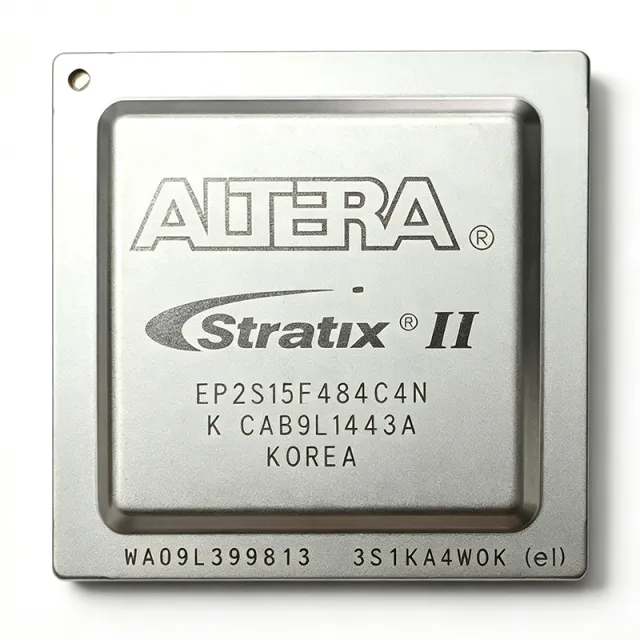
Intel EP2S15F484I4N is a Stratix II field-programmable gate array with 15,600 logic elements, 419,328 bits of embedded memory, 342 I/O pins, and 484-ball fine-pitch ball grid array packaging. Verified distributor data identifies it as a 1.2 V FPGA in the 484-BBGA package, with industrial temperature grading and a 1.2 V supply requirement. Its combination of programmable logic, embedded memory, and high I/O count supports complex digital systems where fixed-function ASICs would be inflexible.
A field-programmable gate array is a programmable semiconductor device built from configurable logic blocks, routing resources, input/output elements, and often embedded memory and DSP-oriented blocks. FPGA devices sit within the broader hierarchy of programmable logic devices, digital integrated circuits, and semiconductors. Engineers configure the logic and interconnect to implement control, communications, interface, and signal-processing functions after fabrication, enabling design changes without a new silicon mask set.
The key electrical and physical characteristics include 15,600 logic elements, 419,328 memory bits, 342 I/O pins, 484 BGA balls, and a 1.2 V operating voltage. The large logic capacity and embedded memory allow parallel digital functions and data buffering within one package. The 342 I/O pins provide broad connectivity for external buses, control signals, and high-speed interfaces. The fine-pitch BGA format supports dense board routing but requires controlled assembly and reliable thermal design.
The device belongs to the Stratix II FPGA family and is associated with 780 configurable logic blocks in the supplied distributor and comparison data. Its architecture is intended for configurable digital implementation rather than fixed application-specific processing. The combination of logic resources and embedded memory can be used for register-intensive designs, protocol handling, state machines, and interface bridging. Exact performance values such as maximum clock frequency, transceiver count, operating temperature limits, package dimensions, and supported I/O standards are not present in the supplied verified text and therefore require datasheet verification.
Typical applications include industrial control, communications equipment, test and measurement, data acquisition, digital signal processing, and embedded systems. The 15,600 logic elements and 419,328 memory bits suit designs requiring substantial programmable logic and local storage, while 342 I/O pins support external memory, converters, processors, and peripheral interfaces. The 484-BBGA package is appropriate for space-constrained systems that need high connection density.
A primary design consideration is that BGA assembly requires precise land-pattern implementation, via-in-pad or escape routing planning, controlled impedance where applicable, and thermal analysis. Before production, confirm pin assignments, voltage tolerances, configuration requirements, clock limits, and industrial temperature limits from the manufacturer datasheet. This page combines verified distributor specifications, compatible-device guidance, comparison parameters, and engineering design considerations to support part selection and BOM review.
견적 요청
문의하기