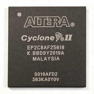
10M50DCF256C7G - MAX 10 FPGA 50K LE, 178 I/O, 256-FBGA | Intel
MPN: 10M50DCF256C7G ✓ Active| Qty | Unit Price | Extended |
|---|---|---|
| 1 | $140.7 | $140.70 |
| 10 | $128.5 | $1,285.00 |
| 100 | $115 | $11,500.00 |
| 250 | $105 | $26,250.00 |
| 500 | $98 | $49,000.00 |
10M50DCF256C7G Overview
An FPGA (Field-Programmable Gate Array) is a class of programmable logic device (PLD) that sits in the hierarchy of digital semiconductors between fixed-function ASICs and microcontrollers. Unlike microcontrollers, which execute software instructions sequentially, FPGAs implement parallel hardware logic that the designer configures via HDL code (Verilog or VHDL). The MAX 10 family specifically targets low-cost, high-volume applications by combining programmable logic with hard IP peripherals, eliminating the need for a separate configuration memory device.
Key features include 16 full-featured 18 x 18 multipliers, 2 PLLs, 288 Kbits of user SRAM, 1.2 V core operation, and support for LVDS, LVCMOS, SSTL, and other single-ended and differential I/O standards. The device is offered in commercial (0C to 85C) temperature grade with the -7 speed grade, optimized for general-purpose logic, glue replacement, and bridging applications.
From an architectural standpoint, the 10M50 uses an SRAM-based LUT-driven fabric backed by on-chip configuration flash, allowing instant-on operation at power-up without external boot devices. The integrated ADC and thermal-sensing diode reduce bill-of-materials cost for industrial control designs that previously required a separate analog companion chip.
Typical applications include industrial motor control, factory automation I/O expansion, video bridging and image aggregation, portable test instruments, and low-cost PCIe endpoint bridging. The non-volatile nature and small 11 x 11 mm BGA footprint make it equally attractive for space-constrained embedded modules.
Designers should pay close attention to the four DDR3/x8 hard memory controller paths on this device, which require strict DQ/DQS group length matching, and to the I/O bank supply grouping (VCCIO per bank) when mixing 1.8 V, 2.5 V, and 3.3 V interfaces on the same chip. Pin assignment with the Quartus Prime Pin Planner is recommended before PCB layout commit.
Drop-in alternatives for 10M50DCF256C7G — same package, pin-to-pin compatible. Different-package parts requiring PCB rework are excluded.
Variants in this series
Same-series models that are drop-in compatible with 10M50DCF256C7G (same form factor and footprint) — differing in Package, Process Technology, Speed Grade, Logic Elements (LE), PLLs.
Quick Comparison Tool — Select alternative parts for side-by-side comparison:
10M50DAF256C7G
✅ Drop-In📋 Reference alternative (not in catalog)
10M50DAF256C8G
✅ Drop-In✓ In Stock
$47.85 / Unit
View Datasheet →10M50DAF256I7G
✅ Drop-In✓ In Stock
$155.2 / Unit
View Datasheet →10M50DCF256A7G
✅ Drop-In✓ In Stock
$29.8 / Unit
View Datasheet →10M50DAF256I6G
✅ Drop-In📋 Reference alternative (not in catalog)
10M40DCF256C7G
✅ Drop-In✓ In Stock
$26.4 / Unit
View Datasheet →10M50DCF256C7G Maximum Ratings & Electrical Characteristics
| Family | MAX 10 |
| Logic Elements (LE) | 50000 |
| Maximum User I/O | 178 |
| User Flash Memory | 1,677,312 bits (1677 Kb) |
| User SRAM | 1638 Kbits |
| Embedded Multipliers (18x18) | 16 |
| PLLs | 2 |
| Global Clock Networks | 20 |
| Process Technology | 55 nm TSMC |
| Core Voltage (VCCINT) | 1.2 V |
| Package | 256-ball FBGA (FineLine BGA) |
| Temperature Grade | Commercial (0C to 85C) |
| Speed Grade | -7 |
| Mounting Type | Surface Mount |
| Configuration Memory | Internal dual-configuration flash (non-volatile) |
| ADC | 12-bit, 1 MSPS, 17 channels (hard IP) |
10M50DCF256C7G 256-ball fbga (fineline bga) Pin Configuration Guide
Pin configuration for 10M50DCF256C7G (256-ball fbga (fineline bga) package). This digital IC includes GPIO, communication interfaces (UART, SPI, I2C), and power pins. Refer to the manufacturer datasheet for alternate pin functions and configuration options. Essential for embedded system design and PCB layout.

No detailed pinout data available for 10M50DCF256C7G.
Refer to the datasheet for full pin configuration.
Typical Applications
10M50DCF256C7G is suitable for 6 applications: Industrial Motor Control, Factory Automation I/O Expansion, Video Bridging and Display Aggregation, Portable Test and Measurement Instruments, Low-Cost PCIe Endpoint Bridging, Glue Logic and Protocol Bridging.
Industrial Motor Control
The 10M50DCF256C7G fits industrial motor control because its 178 GPIO and 16 18x18 hardware multipliers handle three-phase PWM generation and field-oriented control loops without a companion DSP. The 50K LE fabric runs FOC algorithms at 472.5 MHz fabric speed with deterministic single-cycle latency, while the integrated 12-bit 1 MSPS ADC samples current and voltage feedback without an external analog chip. Non-volatile dual-configuration flash enables fail-safe field firmware rollback on motor stalls or watchdog trips. The 256-FBGA package at 11 x 11 mm fits compact servo-drive PCBs, and the 0-85C commercial temperature range covers cabinet-mounted drives.
Recommended
Factory Automation I/O Expansion
In factory-automation I/O-hub designs, the 10M50DCF256C7G serves as a programmable aggregator between Profinet, EtherCAT, or Modbus TCP backbones and 24 V industrial field I/O. The 178 I/O pins multiplex opto-isolated inputs and relay-driver outputs directly, while 2 PLLs generate jitter-free clock trees for deterministic Ethernet timing. 1,677 Kb user flash stores calibration tables, IP-address settings, and machine-ID data that survive power cycles. The integrated 12-bit ADC reads analog sensor inputs (pressure, temperature, flow) on the same silicon, eliminating a separate ADC chip on the BOM.
Recommended
Video Bridging and Display Aggregation
The 10M50DCF256C7G bridges LVDS camera inputs to MIPI-CSI or parallel RGB displays in medical imaging, kiosks, and machine-vision modules. Its 50K LE fabric supports color-space conversion (YUV422 to RGB888) and on-the-fly chroma resampling in hardware pipelines, achieving throughput impossible for microcontrollers at equivalent BOM cost. 16 18x18 multipliers accelerate FIR filters for image preprocessing, while the non-volatile user flash stores factory color-calibration tables. The 256-FBGA package exposes enough LVDS pairs to drive dual 1080p60 streams or a single 4K30 input with reduced blanking.
Recommended
Portable Test and Measurement Instruments
Portable oscilloscope probes, handheld signal analyzers, and field-installable cable testers benefit from the 10M50DCF256C7G's non-volatile boot, low power consumption at 1.2 V VCCINT, and high GPIO density. The 50K LE fabric implements custom DSP filter chains (decimation, FIR, FFT preprocessing) while the 12-bit 1 MSPS internal ADC samples analog test points without a separate ADC. 1,677 Kb of user flash stores instrument calibration constants, operator language strings, and customer-specific test routines that survive battery swaps. The compact 256-FBGA footprint enables handheld form factors below 100 x 60 mm.
Recommended
Low-Cost PCIe Endpoint Bridging
The 10M50DCF256C7G implements PCIe Gen2 x1 endpoint functions on add-in cards and embedded compute modules where cost dominates over lane count. The 50K LE fabric instantiates the PCIe hard IP plus custom DMA engines that move data between host memory and FPGA logic without CPU intervention. Up to 4 hard memory controller paths support DDR3-1600 buffering for high-throughput streaming applications, while the non-volatile flash stores option ROM and configuration bitstream for instant-on enumeration. The 256-FBGA package exposes reference-clock and PCIe lane pins with clean signal-integrity paths when paired with a 4-layer PCB stack-up.
Recommended
Glue Logic and Protocol Bridging
Classic 'glue-logic replacement' is a flagship use case for the 10M50DCF256C7G, where it replaces multiple 74-series logic chips, small CPLDs, and bus-translator ICs in legacy-system refresh designs. The 178 I/O bridge SPI, I2C, UART, parallel bus, and PWM peripherals to a host processor, with 50K LE providing ample headroom for state machines and small FIFOs. The non-volatile instant-on flash eliminates boot-time CPLD-configuration glitches, which is critical in safety-aware industrial controllers. 2 PLLs provide clean clocks for asynchronous domains without external clock-generator ICs.
Recommended
Recommended Products Summary
Engineering reference data for 10M50DCF256C7G — comparison, design guidance, and compliance information.
Selection Guide
Comparison with Alternatives
| Parameter | This Product | 10M50DAF256C7G | 10M50DAF256C8G | 10M50DAF256I7G | 10M40DCF256C7G |
|---|---|---|---|---|---|
| Brand | Intel (formerly Altera) | Intel | Intel | Intel | Intel |
| Package | 256-FBGA (F256) | 256-FBGA (F256) - same | 256-FBGA (F256) - same | 256-FBGA (F256) - same | 256-FBGA (F256) - same |
| Logic Elements | 50000 | 50000 | 50000 | 50000 | 40000 (-20%) |
| Speed Grade | -7 | -7 | -8 (+15% Fmax) | -7 | -7 |
| Temperature Grade | Commercial (0C to 85C) | Commercial (0C to 85C) | Commercial (0C to 85C) | Industrial (-40C to 100C) | Commercial (0C to 85C) |
| User I/O | 178 | 178 | 178 | 178 | 178 |
| User Flash | 1,677 Kb | 1,677 Kb | 1,677 Kb | 1,677 Kb | 1,260 Kb |
| Embedded 18x18 Multipliers | 16 | 16 | 16 | 16 | 16 |
| Pin-to-Pin Compatible | Reference | Yes | Yes | Yes | Yes |
Key Differentiators
- Same-die commercial-grade option at lower cost (vs 10M50DAF256I7G)
- Speed grade -7 is the mainstream sweet spot (vs 10M50DAF256C8G)
- Full 50K LE vs cost-down 40K LE (vs 10M40DCF256C7G)
Design Notes
The 256-FBGA package uses 0.8 mm ball pitch; route the PCB with at least 4 layers and 0.4 mm via-in-pad (VIPPO) or microvia structures to fan out the inner balls. According to MAX 10 hardware-design guidelines, all VCCINT and VCCA pins require decoupling within 100 mils of the BGA balls, and at least one 100 uF bulk capacitor is recommended per rail. The exposed-pad thermal slug (if present on F256) must be soldered to a 4 x 4 thermal pad with stitched vias to the inner ground plane for 1.5 W dissipation headroom.
Estimated: power budget at maximum fabric utilization of 50K LE, 472.5 MHz toggle, and 178 GPIO switching at 100 MHz is approximately 1.2 W core plus I/O. Plan for at least a 2 W PCB thermal budget to keep junction below 85C in a sealed enclosure. Avoid the common mistake of leaving JTAG TCK/TMS/TDO/DATA pins floating: MAX 10 expects 4.7 kohm pull-ups on TMS and TDI per the device handbook to enter configuration mode reliably.
DDR3 controller pins are assigned to specific DQ/DQS groups; the Quartus Prime Pin Planner must be consulted before layout commit, because post-layout pin reassignment is impossible for hard memory controllers. Use 100-ohm differential routing for LVDS pairs and keep trace length mismatch below 50 mils. Place the 50 MHz or 100 MHz reference clock within 200 mils of the CLK pin and shield it from GPIO switching noise with a guard ring tied to ground.
Compliance Information
RoHS and REACH compliance per Altera/Intel product environmental reporting. AEC-Q100 is not applicable as this is an industrial/commercial-grade FPGA, not an automotive-qualified part; the -I temperature grade variant is not the same as AEC-Q100 qualification.