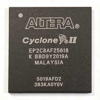
EP1K30FC256-3NAA - ACEX-1K FPGA, 30K Gate, 171 I/O | Intel
MPN: EP1K30FC256-3NAA ✗ End of Life| Qty | Unit Price | Extended |
|---|---|---|
| 1 | $18.75 | $18.75 |
| 10 | $16.1 | $161.00 |
| 100 | $14.3 | $1,430.00 |
| 500 | $12.9 | $6,450.00 |
| 1,000 | $11.5 | $11,500.00 |
EP1K30FC256-3NAA Overview
An FPGA is a semiconductor logic device whose internal architecture can be configured after manufacturing. Unlike a fixed ASIC, an FPGA contains programmable look-up tables, register elements, and routing fabrics that are loaded from external configuration memory every time the part powers up. The ACEX-1K family belongs to the high-density programmable-logic hierarchy: FPGA -> programmable logic device -> embedded integrated circuit. It is commonly used where moderate logic density, parallel I/Os, and redesign flexibility are needed at system level.
Key features of the EP1K30FC256-3NAA include 1728 logic elements for combinatorial and sequential logic, 171 parallel user I/Os that simplify bus interfaces and data acquisition systems, 24576 embedded RAM bits for small FIFOs and register files, and a 0.22 um 2.5 V architecture. The 256-ball FineLine BGA package provides a compact surface-mount footprint while maintaining adequate I/O count for card-edge or mezzanine systems.
The ACEX-1K architecture implements logic in a matrix of LABs and uses embedded array blocks for memory. Being SRAM-based, the FPGA needs an external configuration device such as an EPC2 or a host processor to download a bitstream at power-up. The same-frame migration feature in ACEX-1K 256-ball packages allows different density grades to share a common BGA land pattern, easing design reuse across lower and higher density EP1K variants.
Typical applications include industrial I/O glue logic, communication-protocol bridging, data-acquisition control, video timing and display interface logic, embedded processor bus bridges, and legacy FPGA replacement for boards using ACEX-1K devices. The 171 I/Os give enough channels for parallel peripherals, while the 2.5 V core lowers switching power compared with older 5 V FPGA families.
A key design consideration is configuration management: because ACEX-1K has no nonvolatile internal flash, the designer must ensure the configuration source is reliable and that I/O pins are not actively driving before configuration is complete. Decoupling each VCC and VCCIO ball with a 0.1 uF ceramic capacitor is also required for stable high-speed operation.
This page consolidates distributor stock status, pin-compatible ACEX-1K alternatives, ordering-code guidance, and practical board-level notes that are not all present in the original manufacturer datasheet. Pricing and availability are reported as of 2026-09-07 from public distributor listings.
Drop-in alternatives for EP1K30FC256-3NAA — same package, pin-to-pin compatible. Different-package parts requiring PCB rework are excluded.
Variants in this series
Same-series models that are drop-in compatible with EP1K30FC256-3NAA (same form factor and footprint) — differing in Speed Grade, Package, Process Technology, Core Supply Voltage, Logic Elements.
Quick Comparison Tool — Select alternative parts for side-by-side comparison:
EP1K30FC256-3N
✅ Drop-In✓ In Stock
$17.5 / Unit
View Datasheet →EP1K30FC256-3
✅ Drop-In✓ In Stock
$11.1 / Unit
View Datasheet →EP1K30FC256-2N
✅ Drop-In✓ In Stock
$21.45 / Unit
View Datasheet →EP1K30FC256-2
✅ Drop-In ⚠️ Specs Unverified✓ In Stock
$22.95 / Unit
View Datasheet →EP1K30FC256-1N
✅ Drop-In ⚠️ Specs Unverified✓ In Stock
$13.95 / Unit
View Datasheet →EP1K30FC256-1
✅ Drop-In✓ In Stock
$17.85 / Unit
View Datasheet →EP1K30FI256-2N
✅ Drop-In✓ In Stock
$18.4 / Unit
View Datasheet →EP1K30FC256-3NAA Maximum Ratings & Electrical Characteristics
| Product Category | FPGA - Field Programmable Gate Array |
| Family | ACEX-1K |
| Number of Logic Elements | 1728 |
| Number of Gates | 30000 (30K) |
| Embedded RAM Bits | 24576 bits |
| Number of User I/Os | 171 |
| Maximum Internal Clock Frequency | 200 MHz |
| Core Supply Voltage | 2.5 V |
| IC Process Technology | 0.22 um |
| Package Type | 256-ball FBGA (FineLine BGA) |
| Package Form | 256-BBGA |
| Mounting Type | Surface Mount |
| Speed Grade | -3 (ordering code) |
| Configuration Type | SRAM-based, external configuration device required |
EP1K30FC256-3NAA 256-bbga Pin Configuration Guide
Pin configuration for EP1K30FC256-3NAA (256-bbga package). This digital IC includes GPIO, communication interfaces (UART, SPI, I2C), and power pins. Refer to the manufacturer datasheet for alternate pin functions and configuration options. Essential for embedded system design and PCB layout.

No detailed pinout data available for EP1K30FC256-3NAA.
Refer to the datasheet for full pin configuration.
Typical Applications
EP1K30FC256-3NAA is suitable for 6 applications: Industrial I/O Glue Logic and Legacy Control Cards, Communication Protocol Bridge and Parallel Interface Logic, Data Acquisition and Instrumentation Front-End Control, Video Timing and Display Interface Control, Embedded Processor Bus Bridge and Memory Interface, Legacy FPGA Replacement and Long-Term Service Support.
Industrial I/O Glue Logic and Legacy Control Cards
The EP1K30FC256-3NAA is a strong fit for industrial I/O cards where 171 user I/Os allow direct connection of limit switches, sensor banks, relay drivers, and status LED arrays. Because ACEX-1K devices are 2.5 V FPGAs built on a 0.22 um process, they can replace older board-level logic with a single compact package while preserving the existing 256-ball layout. For legacy PLC and machine-control boards, this reduces many discrete 74-series devices to one programmable part. The 1728 logic elements are sufficient for several hundred simple state-machine and combinatorial logic equations, but they are not intended to hold processor cores or large soft IP. Place the FPGA close to the backplane connector, decouple each supply ball with 0.1 uF ceramics, and use an EPC2 configuration device for automatic power-up loading. This approach keeps the wiring simple and the system performance deterministic.
Recommended
Communication Protocol Bridge and Parallel Interface Logic
Communication systems often need to translate between different parallel buses or insert small protocol-state machines between line interfaces and host controllers. The EP1K30FC256-3NAA supports 171 parallel I/Os and a 200 MHz internal clock, making it useful for MII-style bus gaskets, address decoding, and serial/parallel conversion without burdening the host CPU. The 24576 RAM bits can buffer short packets or serve as small FIFOs between clock domains. Because the device is SRAM-based, the configuration bitstream can be downloaded by a system processor instead of a separate flash device, reducing board height in compact networking modules. To use it successfully, assign I/O pins against the PCB route and avoid overloading the 2.5 V core supply with excessive simultaneous switching output pins. A straightforward design can be implemented in fewer than 1728 logic elements, leaving spare resources for protocol status registers.
Recommended
Data Acquisition and Instrumentation Front-End Control
For data acquisition boards, the EP1K30FC256-3NAA provides a programmable timing engine that coordinates analog-to-digital converters, sample-and-hold circuits, and FIFO readout. Its 171 I/Os are enough to connect multiple 16-bit ADC buses with separate control lines, while the 24576 RAM bits can act as a small sample buffer before DMA transfer to a host processor. The 2.5 V core and 0.22 um process help limit digital switching noise on the analog side compared to older 5 V programmable logic. However, because the ACEX-1K is not a low-noise analog part, route digital traces away from sensitive analog input lines and add solid ground stitching. Designers can implement ADC state machines, channel counters, and simple DSP pre-processing in the 1728 logic elements. This makes the FPGA well suited to industrial data loggers, vibration monitors, and laboratory instrumentation retrofits.
Recommended
Video Timing and Display Interface Control
The EP1K30FC256-3NAA can generate pixel clocks, blanking intervals, synchronization pulses, and memory-address sequences for video display controllers. With 1728 logic elements, it is not an appropriate place to implement a large video scaler, but it can handle timing generation, line buffering, and level adaptation between a video decoder and a display panel. The 24576 RAM bits allow a few full-color line buffers at moderate resolutions, and the 171 I/Os connect to parallel RGB buses and control registers. The 256-FBGA package is convenient for multi-layer display boards where routing density is high. Use a separate low-jitter clock source for pixel timing and keep the FPGA global clock network free from noisy digital outputs. For legacy imaging systems, this FPGA is a practical way to re-implement discontinued timing ASICs without a PCB redesign.
Recommended
Embedded Processor Bus Bridge and Memory Interface
Embedded systems sometimes require an address-decode and bus-bridge chip that connects a microprocessor to several memory-mapped peripherals. The EP1K30FC256-3NAA can implement chip selects, interrupt routing, wait-state generation, and read/write strobe translation in programmable logic. Because it has 171 I/Os and a 2.5 V core, it can sit between a 3.3 V host bus and multiple peripheral banks without needing dozens of external drivers. The 24576 RAM bits can form small command queues or register scratchpads. This type of design is well within the capacity of 1728 logic elements when implemented with simple state machines. One important caution is to avoid placing high-speed processor buses too far from the BGA: keep trace lengths matched and add series termination near the FPGA to reduce reflections. A configuration device or host-driven download should be provided for every power-up cycle.
Recommended
Legacy FPGA Replacement and Long-Term Service Support
For boards that must continue production after the original ACEX-1K device has become difficult to source, the EP1K30FC256-3NAA is valuable because it uses the same 256-FBGA package and pin-compatible ACEX-1K footprint used by several EP1K30 variants. The 1728 logic elements, 24576 RAM bits, and 171 user I/Os are identical across the FC256 speed-grade family, so a validated -3 bitstream can usually be ported to EP1K30FC256-3N. When complete replacement parts are exhausted, this FPGA can also serve as the starting point for moving a legacy design to a newer Intel/Altera family, but that migration requires a new pinout because newer FPGAs are not pin compatible with ACEX-1K. For service-support suppliers, keeping the original Quartus II project, configuration file, and BSDL file is essential for reproducing the same timing and pin assignment.
Recommended
Recommended Products Summary
Engineering reference data for EP1K30FC256-3NAA — comparison, design guidance, and compliance information.
Selection Guide
Comparison with Alternatives
| Parameter | This Product | EP1K30FC256-3N | EP1K30FC256-2N | EP1K30FI256-2N |
|---|---|---|---|---|
| Brand | Intel (Altera) | Intel (Altera) | Intel (Altera) | Intel (Altera) |
| Package | 256-BGA | 256-BGA | 256-BGA | 256-BGA |
| Logic Elements | 1728 | 1728 | 1728 | 1728 |
| Gates | 30000 | 30000 | 30000 | 30000 |
| RAM Bits | 24576 | 24576 | 24576 | 24576 |
| User I/O | 171 | 171 | 171 | 171 |
| Core Voltage | 2.5 V | 2.5 V | 2.5 V | 2.5 V |
| Speed Grade | -3NAA | -3N | -2N | -2N |
Key Differentiators
- Maintains legacy ACEX-1K 256-FBGA land pattern with verified distributor availability (vs EP1K30FC256-3N)
- Conservative -3 speed grade gives more timing margin for legacy board routes (vs EP1K30FC256-2N)
- Same-frame migration path across the ACEX-1K 256-ball package family (vs EP1K30FC256-1N)
Design Notes
The EP1K30FC256-3NAA is an SRAM-based FPGA, so it will not retain its configuration after power-down. You must provide a configuration device such as an EPC2 or download the bitstream from a host processor at every power-up. Follow the Intel/Altera ACEX-1K configuration guidelines: hold nCONFIG low until supplies are stable, drive DCLK with the correct voltage threshold, then release nCONFIG to start configuration. I/O pins should be tri-stated during configuration to prevent bus contention with other devices on the same net.
Power the 2.5 V core through a low-impedance supply plane rather than a thin trace. Place one 0.1 uF ceramic capacitor close to every VCC and VCCIO ball, and add a 10 uF bulk capacitor at the FPGA supply entry. If the design includes many simultaneously switching outputs, estimate the supply current with the Quartus II power estimator and verify the voltage regulator can handle transient current. In legacy boards, the original ACEX-1K may have been powered by an older 2.5 V linear regulator; verify that regulator still meets the worst-case current.
The EP1K30FC256-3NAA is a 256-ball FineLine BGA with 171 user I/Os. Use a dense via-in-pad or microvia stack-up for fanout, and assign FPGA pins in Quartus II after performing a rough PCB route review. Keep clock inputs on dedicated global clock pins where possible and use series termination near the BGA for high-speed point-to-point signals. Avoid placing sensitive analog inputs near heavily switching FPGA outputs; use ground guard traces or separate ground stitch vias if mixed-signal circuits share the same board.
Compliance Information
Compliance status was not stated in the verified distributor snippets. Altera legacy ordering codes with N often indicate Pb-free finish, but RoHS status should be confirmed against the manufacturer PCN and the actual date/lot code before claiming compliance.