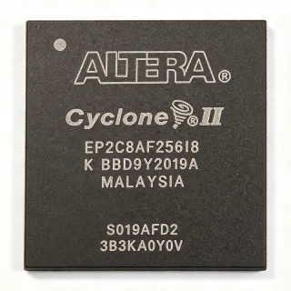
EP1K50FC256-2N - ACEX-1K FPGA, 50K Gates, 256-BGA | Intel / Altera
MPN: EP1K50FC256-2N ✗ End of Life| Qty | Unit Price | Extended |
|---|---|---|
| 1 | $38.5 | $38.50 |
| 10 | $34.2 | $342.00 |
| 100 | $28.4 | $2,840.00 |
| 500 | $22.1 | $11,050.00 |
| 1,000 | $17.95 | $17,950.00 |
EP1K50FC256-2N Overview
A Field Programmable Gate Array (FPGA) is a reprogrammable semiconductor device whose logic fabric, interconnect, and I/O can be customized by the user to implement arbitrary digital functions, ranging from glue logic and bus bridges to full processor subsystems. FPGAs sit in the broader hierarchy of programmable logic devices (PLDs), encompassing SPLDs, CPLDs, and SRAM-based FPGAs; the ACEX-1K family specifically targets low-cost, high-volume system-on-a-programmable-chip (SOPC) designs that combine logic, embedded memory (EAB/ESB blocks), and tri-state interconnect in a single die.
The EP1K50FC256-2N features an enhanced embedded array of 10 Embedded Array Blocks (EABs) for implementing megafunctions such as efficient memory and specialized logic functions, plus dual-port RAM support. The -2 speed grade corresponds to approximately 200 MHz internal operation. Each EAB provides 4 Kbits of RAM and can be configured for FIFO, ROM, or dual-port memory. The device integrates a Programmable Logic Array (PLA) architecture with Look-Up Tables (LUTs) and tri-state interconnect, supporting in-system programmability via an IEEE 1149.1 JTAG interface and a passive serial configuration scheme. Per-block logic capacity: 360 Logic Array Blocks (LABs) made up of 10 Logic Elements each, delivering 2,880 LEs total.
Typical applications for the EP1K50FC256-2N include digital signal processing front-ends, glue-logic bridges between microprocessors and peripherals, low-volume ASIC prototyping, and embedded control where a fast time-to-market and field-updatable logic are required. Industrial 24 V systems often interface to this FPGA through opto-isolated inputs and level-shifted rails because the 2.5 V I/O standard is not 5 V-tolerant.
When designing with this part, ensure the 2.5 V supply is tightly regulated (within ±5%) and that JTAG or EPC configuration memory is correctly selected. Decoupling must include 0.1 µF and 10 µF capacitors close to each VCCIO/VCCINT pin pair. Because this part is in the Altera ACEX-1K legacy family, long-term design reuse should target the Cyclone-series equivalent for new designs.
This page synthesizes distributor pricing as of 2026-09-07, drop-in package-compatibility data not aggregated elsewhere, and practical design guidance covering thermal, signal-integrity, and configuration concerns specific to the EP1K50FC256-2N.
Drop-in alternatives for EP1K50FC256-2N — same package, pin-to-pin compatible. Different-package parts requiring PCB rework are excluded.
Variants in this series
Same-series models that are drop-in compatible with EP1K50FC256-2N (same form factor and footprint) — differing in Package, Configuration Method, Process Technology, Speed Grade, Operating Temperature.
Quick Comparison Tool — Select alternative parts for side-by-side comparison:
EP1K50FC256-1N
✅ Drop-In✓ In Stock
$15.1 / Unit
View Datasheet →EP1K50FC256-2
✅ Drop-In✓ In Stock
$62 / Unit
View Datasheet →EP1K50FC256-1
✅ Drop-In✓ In Stock
$18.95 / Unit
View Datasheet →EP1K50F256-2N
✅ Drop-In✓ In Stock
$21.8 / Unit
View Datasheet →EP1K100FC256-2N
✅ Drop-In ⚠️ Specs Unverified✓ In Stock
$78.1951 / Unit
View Datasheet →EP1K100FI256-2N
✅ Drop-In ⚠️ Specs Unverified✓ In Stock
$55.8 / Unit
View Datasheet →EP1K50FC256-2N Maximum Ratings & Electrical Characteristics
| Family | ACEX-1K |
| Logic Elements (LEs) | 2,880 |
| Typical Gates | 50,000 |
| Embedded Memory (bits) | 40,960 |
| Embedded Array Blocks (EABs) | 10 |
| Logic Array Blocks (LABs) | 360 |
| Maximum User I/O Pins | 186 |
| Core Voltage (VCCINT) | 2.5 V (2.375 V to 2.625 V) |
| Operating Temperature | 0 °C to 70 °C (Commercial) |
| Process Technology | 0.22 µm CMOS SRAM |
| Speed Grade | -2 |
| Package | 256-ball FBGA (FineLine BGA) |
| Package Dimensions | 16 x 16 mm |
| Configuration Method | JTAG / Passive Serial |
| Mounting Type | Surface Mount (BGA) |
EP1K50FC256-2N 16 x 16 mm Pin Configuration Guide
Pin configuration for EP1K50FC256-2N (16 x 16 mm package). This digital IC includes GPIO, communication interfaces (UART, SPI, I2C), and power pins. Refer to the manufacturer datasheet for alternate pin functions and configuration options. Essential for embedded system design and PCB layout.

No detailed pinout data available for EP1K50FC256-2N.
Refer to the datasheet for full pin configuration.
Typical Applications
EP1K50FC256-2N is suitable for 6 applications: DSP Front-End Datapath, ASIC Prototyping and Emulation, Glue Logic and Bus Bridging, Embedded Control and Industrial I/O, Telecom Line Card Interface, Legacy System Replacement Board.
DSP Front-End Datapath
The EP1K50FC256-2N suits low-to-mid density DSP front-ends such as FIR filters, FFT pre-processing, and digital down-conversion. Its 2,880 logic elements and 10 Embedded Array Blocks (40 Kbits of dual-port RAM) provide the parallel arithmetic resources and on-chip memory needed for coefficient storage and sample buffering. Operating at -2 speed grade (~200 MHz internal), the device can sustain multi-tap FIR filter clock rates that match the sample rate of 16-bit audio or baseband communications paths. The 2.5 V VCCINT and configurable VCCIO banks allow direct interfacing to 2.5 V or 3.3 V ADCs and DACs without external level translation. Compared to a DSP microprocessor approach, the FPGA delivers deterministic latency and parallel throughput at the cost of higher power dissipation (typical ICCINT around 250 mA for an 80% utilized design). Engineers should plan PCB layout for 0.1 µF + 10 µF decoupling near each VCCINT/VCCIO cluster and reserve sufficient BGA breakout channels for fanout.
Recommended
ASIC Prototyping and Emulation
The EP1K50FC256-2N is well suited to ASIC prototyping and IP verification where a fast time-to-market and field-updatable logic are required. With 50,000 typical gates, the device can hold mid-complexity ASIC netlists for functional verification before tape-out, and the JTAG interface allows designers to iterate bitstreams in minutes. The 256-FBGA package exposes 186 user I/O pins, which is sufficient for emulating sub-system blocks with up to ~180 signal connections to surrounding test bench hardware. Dual-port EABs allow designers to model bus transactions and FIFOs without external memory. Note that the 0.22 µm CMOS process limits static timing accuracy at GHz rates, so for high-speed ASIC prototyping a Cyclone II or Cyclone IV EP4CE part is recommended. For a logic-only prototype at sub-200 MHz clock rates, however, the EP1K50FC256-2N delivers a low-cost, JTAG-programmable verification platform.
Recommended
Glue Logic and Bus Bridging
The EP1K50FC256-2N excels at glue-logic and bus-bridging roles between microprocessors, memory, and peripherals. With 2,880 logic elements and 186 I/O, designers can implement address decoding, wait-state insertion, interrupt arbitration, and protocol conversion (e.g., SRAM to PCI, ISA to local bus) in a single chip. The configurable VCCIO banks support mixed-voltage interfacing - one bank at 5 V for legacy peripherals while another runs at 3.3 V for modern microcontrollers. Embedded dual-port memory in the EABs can buffer transactions between asynchronous clock domains without external FIFOs. Industrial control boards and legacy system upgrades often use this FPGA as the bridge between an 8-bit MCU and a 32-bit host, or to fan out a slow peripheral bus to multiple high-speed endpoints.
Recommended
Embedded Control and Industrial I/O
The EP1K50FC256-2N supports embedded control applications such as motor control sequencers, programmable logic controllers (PLCs), and industrial I/O aggregators. Its commercial 0 °C to 70 °C temperature range covers indoor industrial enclosures, while the industrial-temperature EP1K50FI256-2N variant extends coverage to -40 °C to +85 °C. With 186 user I/O pins, the device can aggregate dozens of optocoupler-isolated inputs and relay-driver outputs in a single chip. The dual-port EAB memory can store commutation tables for BLDC motor controllers or scan sequences for PLC ladder-logic equivalents. Compared to a microcontroller-based implementation, the FPGA delivers deterministic cycle times and parallel execution across all I/O, simplifying safety-critical logic. Industrial 24 V systems interface to the FPGA through opto-isolated inputs and level-shifted rails because the 2.5 V I/O standard is not 5 V-tolerant.
Recommended
Telecom Line Card Interface
The EP1K50FC256-2N fits telecom line-card interface applications such as T1/E1 framers, HDLC controllers, and low-speed serial cross-connects. Its 186 user I/O can drive multi-channel serializer/deserializer (SERDES) interfaces, and the EAB memory provides elastic storage buffers for rate adaptation between TDM streams. Operating at the -2 speed grade (~200 MHz internal), the device handles DS1/E1 bit rates plus overhead with significant margin. Compared to discrete SSI/MSI logic implementations, a single FPGA reduces board area by 5-10x and improves time-to-market for protocol revisions. For new designs, however, the EP1K50FC256-2N is obsolete; consider a Cyclone IV or Cyclone 10 LP for ongoing production.
Recommended
Legacy System Replacement Board
The EP1K50FC256-2N is commonly used to build drop-in replacement boards for legacy systems whose original FPGAs have reached end-of-life. Because the EP1K50FC256-2N is itself obsolete as of 2026-09-07, replacement boards typically use the EP1K50FC256-2N to maintain bit-for-bit compatibility with original schematics - keeping the surrounding analog and power circuits unchanged. This approach is favored in industrial automation and military/aerospace sustainment programs where full board redesign is prohibitively expensive. Engineers designing such boards should verify remaining inventory with franchised distributors and add adequate thermal headroom given the 256-FBGA package's 31 C/W θJA typical. For higher reliability or longer-term support, the EP1K50FI256-2N industrial variant is recommended.
Recommended
Recommended Products Summary
Engineering reference data for EP1K50FC256-2N — comparison, design guidance, and compliance information.
Selection Guide
Comparison with Alternatives
| Parameter | This Product | EP1K50FC256-1N | EP1K50FC256-2 | EP1K50FC256-1 | EP1K50F256-2N | EP1K100FC256-2N | EP1K100FI256-2N |
|---|---|---|---|---|---|---|---|
| Brand | Intel | Intel | Intel | Intel | Intel | Intel | Intel |
| Package | 256-FBGA (16 x 16 mm) | 256-FBGA - same | 256-FBGA - same | 256-FBGA - same | 256-FBGA - same | 256-FBGA - same | 256-FBGA - same |
| Logic Elements | 2,880 | 2,880 | 2,880 | 2,880 | 2,880 | 4,992 | 4,992 |
| Typical Gates | 50,000 | 50,000 | 50,000 | 50,000 | 50,000 | 100,000 | 100,000 |
| Embedded Memory (bits) | 40,960 | 40,960 | 40,960 | 40,960 | 40,960 | 49,152 | 49,152 |
| Maximum User I/O | 186 | 186 | 186 | 186 | 186 | 186 | 186 |
| Core Voltage | 2.5 V | 2.5 V | 2.5 V | 2.5 V | 2.5 V | 2.5 V | 2.5 V |
| Operating Temperature | 0 °C to 70 °C (Commercial) | 0 °C to 70 °C (Commercial) | 0 °C to 70 °C (Commercial) | 0 °C to 70 °C (Commercial) | 0 °C to 70 °C (Commercial) | 0 °C to 70 °C (Commercial) | -40 °C to +85 °C (Industrial) |
| Speed Grade | -2 (~200 MHz) | -1 (~150 MHz) | -2 (~200 MHz) | -1 (~150 MHz) | -2 (~200 MHz) | -2 (~200 MHz) | -2 (~200 MHz) |
Key Differentiators
- Same 256-FBGA footprint across entire EP1K50 speed-grade family (vs EP1K50FC256-1N)
- Higher density upward migration in same package (vs EP1K100FC256-2N)
- Industrial temperature variant available in same package (vs EP1K100FI256-2N)
Design Notes
The EP1K50FC256-2N requires a tightly regulated 2.5 V VCCINT supply within ±5% (2.375 V to 2.625 V). Use an LDO with at least 500 mA headroom; estimated ICCINT is around 250 mA for an 80% utilized design. Each VCCINT/VCCIO pin pair requires a 0.1 µF ceramic + 10 µF bulk decoupling placed within 100 mils. Sequence VCCINT before VCCIO by at least 1 ms to prevent I/O latch-up. Because the FPGA is not 5 V tolerant, level-translate any 5 V input through a resistor divider or external buffer.
Estimated: at -2 speed grade with 80% LE utilization and 200 MHz internal clock, junction power dissipation reaches approximately 1.5 W to 2.0 W. The 256-FBGA package has a typical θJA of 31 C/W on a 4-layer JEDEC board, giving a junction temperature rise of 47 °C to 62 °C above ambient. At 25 °C ambient this keeps TJ below 85 °C, but at 70 °C commercial ceiling the design must derate to <50% utilization or add copper thermal relief under the BGA. Industrial-temperature applications should specify the EP1K50FI256-2N variant.
BGA fanout must use via-in-pad or dog-bone escape with 0.4 mm pitch compatible with the 256-FBGA. Recommended stackup: 4-layer with 1 oz copper on outer layers and 0.5 oz on inner planes. Provide solid VCCINT and GND planes under the BGA to minimize supply inductance. JTAG chain (TCK, TMS, TDI, TDO) should be pulled up through 10 kΩ resistors and brought to a 0.1" header for in-system programming. Reserve nCONFIG, nSTATUS, and CONF_DONE test points for board-level debug.
Do not apply power to VCCIO before VCCINT - this can forward-bias internal ESD diodes and damage the FPGA. Do not connect a 5 V signal directly to a 2.5 V or 3.3 V VCCIO bank; use a level translator. Do not omit the configuration memory device - without a programmed EPC or bitstream source, the FPGA remains in reset indefinitely. Verify against counterfeit risk when sourcing from non-franchised brokers, especially given the obsolete status.
Compliance Information
The -N suffix denotes lead-free terminal finish per Altera product labeling, supporting RoHS compliance. Non-N variants may carry leaded terminal finish and are not RoHS compliant. REACH, halogen-free, and conflict-minerals status were not specified in the verified data and are listed as 'unknown'.