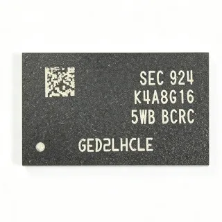
27C512-20HW - 512Kbit CMOS EPROM 200ns LCC32 | Fujitsu
MPN: 27C512-20HW ✗ End of Life| Qty | Unit Price | Extended |
|---|---|---|
| 1 | $4.5 | $4.50 |
| 10 | $4.05 | $40.50 |
| 100 | $3.6 | $360.00 |
| 500 | $3.15 | $1,575.00 |
| 1,000 | $2.7 | $2,700.00 |
Drop-in alternatives for 27C512-20HW — same package, pin-to-pin compatible. Different-package parts requiring PCB rework are excluded.
Quick Comparison Tool — Select alternative parts for side-by-side comparison:
27C512-20FA
✅ Drop-In✓ In Stock
$1.85 / Unit
View Datasheet →27C512-20
✅ Drop-In✓ In Stock
$4.1 / Unit
View Datasheet →27C512-25
✅ Drop-In✓ In Stock
$3.2 / Unit
View Datasheet →27C512L-15T
✅ Drop-In✓ In Stock
Contact for price
View Datasheet →M27C512
✅ Drop-In📋 Reference alternative (not in catalog)
AT27C512
✅ Drop-In📋 Reference alternative (not in catalog)
TMS27C512
✅ Drop-In📋 Reference alternative (not in catalog)
SST27SF512
✅ Drop-In📋 Reference alternative (not in catalog)
27C512-20HW Maximum Ratings & Electrical Characteristics
| Memory Size | 512 Kbit (64K x 8) |
| Memory Type | CMOS EPROM (UV / OTP) |
| Access Time | 200 ns |
| Supply Voltage | 5 V +/-10% |
| Standby Current | 20 uA typical (CMOS standby) |
| Organization | 64K x 8 bit |
| Programming Algorithm | 100% Flashrite programming |
| Pinout | JEDEC-approved EPROM pinout |
| Outputs | Tri-state, O0 to O7 |
| Control Signals | CE (active-low), OE (active-low) |
| Package | LCC32 (32-lead chip carrier) |
| Mounting Type | Surface Mount |
| Erase Method | UV erase (UV variant) / OTP (windowless variant) |
| Manufacturer | Fujitsu |
27C512-20HW Pin Configuration
| Pin 1 | A15 — Address input bit 15 |
| Pin 2 | A12 — Address input bit 12 |
| Pin 3 | A7 — Address input bit 7 |
| Pin 4 | A6 — Address input bit 6 |
| Pin 5 | A5 — Address input bit 5 |
| Pin 6 | A4 — Address input bit 4 |
| Pin 7 | A3 — Address input bit 3 |
| Pin 8 | A2 — Address input bit 2 |
| Pin 9 | A1 — Address input bit 1 |
| Pin 10 | A0 — Address input bit 0 |
| Pin 11 | O0 — Data output bit 0 (tri-state) |
| Pin 12 | O1 — Data output bit 1 (tri-state) |
| Pin 13 | O2 — Data output bit 2 (tri-state) |
| Pin 14 | GND — Ground |
| Pin 15 | O3 — Data output bit 3 (tri-state) |
| Pin 16 | O4 — Data output bit 4 (tri-state) |
| Pin 17 | O5 — Data output bit 5 (tri-state) |
| Pin 18 | O6 — Data output bit 6 (tri-state) |
| Pin 19 | O7 — Data output bit 7 (tri-state) |
| Pin 20 | CE — Chip Enable (active-low) |
| Pin 21 | A10 — Address input bit 10 |
| Pin 22 | OE — Output Enable (active-low) |
| Pin 23 | A11 — Address input bit 11 |
| Pin 24 | A9 — Address input bit 9 |
| Pin 25 | A8 — Address input bit 8 |
| Pin 26 | A13 — Address input bit 13 |
| Pin 27 | A14 — Address input bit 14 |
| Pin 28 | NC — Not connected (per datasheet) |
| Pin 29 | PGM — Program enable (active-low, programming mode) |
| Pin 30 | NC — Not connected (per datasheet) |
| Pin 31 | VPP — Programming supply voltage (programming mode) |
| Pin 32 | VCC — Power supply +5 V |
Safe Operating Area (SOA) & Thermal Characteristics
No official SOA curve available for this digital IC. Always operate within absolute maximum ratings specified in the datasheet. Ensure adequate cooling and derate as needed.
Typical Applications
27C512-20HW is suitable for 6 applications: Automotive ECU Firmware (OBD-I Era), Industrial Controller Firmware Storage, Arcade Boards and Retro Computing, Telecom Line Cards and Network Equipment, Test and Measurement Instrument Firmware, Embedded Systems New-Old-Stock Retrofits.
Automotive ECU Firmware (OBD-I Era)
The 27C512 is the classic EPROM of OBD-I engine control units, where a single 64K x 8 chip holds the fuel and ignition maps. The 27C512-20HW fits the standard 32-pin PLCC/LCC socket on these boards, and its 200 ns access time meets the 8-16 bit processor bus timing of that era. Its JEDEC pinout means Atmel AT27C512 or SST27SF512 devices can be substituted for tuning iterations, while genuine EPROMs keep the production ECU read-compatible. Performance consideration: verify date-code authenticity, since counterfeit EPROMs with erased or mislabeled dies are common in this market and can corrupt map data or fail at temperature.
Recommended
Industrial Controller Firmware Storage
Legacy PLCs, motor drives, and industrial single-board computers store boot code and application firmware in 27C512 EPROM sockets. The 27C512-20HW provides 512 Kbit of truly non-volatile storage immune to accidental overwrites, with only 20 uA typical standby current from the CMOS process - valuable in battery-backed controller configurations. Its 5 V supply with +/-10% tolerance tolerates noisy industrial 5 V rails, and tri-state outputs simplify memory-bus sharing with RAM and I/O. Design consideration: industrial environments with marginal power sequencing favor EPROM's hard-wired immunity over Flash, and replacements should match the original 200 ns (or faster) speed grade to preserve worst-case bus timing at temperature.
Recommended
Arcade Boards and Retro Computing
Arcade PCBs, home computers, and game consoles of the late 1980s and 1990s use 27C512 devices for game code and character ROMs. The 27C512-20HW LCC32 variant suits the surface-mounted ROM sockets on JAMMA-era boards, while its 200 ns speed supports the 68000 and Z80 buses of that hardware. Repair shops value the JEDEC-approved pinout, which lets one programmer and one socket profile serve Fujitsu, ST M27C512, and TI TMS27C512 parts interchangeably. Performance consideration: for boards with tight ROM access timing, prefer a 150 ns grade such as 27C512L-15T; for code storage with occasional updates, SST27SF512 simplifies development without socket rework.
Recommended
Telecom Line Cards and Network Equipment
Central-office line cards, modems, and early network equipment shipped with 27C512 EPROMs holding DSP code and protocol firmware. The 27C512-20HW matches these designs with 64K x 8 organization, a single 5 V rail, and low CMOS standby power suited to densely populated cards. CE and OE control allow multiple EPROMs to share a backplane data bus with clean tri-state isolation, and the LCC32 surface-mount package withstands vibration better than DIP sockets. Design consideration: telecom racks often impose extended temperature ranges, so confirm the operating range against the original system specification and prefer industrial-temperature stock when available from excess distributors.
Recommended
Test and Measurement Instrument Firmware
Oscilloscopes, logic analyzers, and bench power supplies of the 1990s store monitor firmware and calibration tables in 27C512 sockets. The 27C512-20HW offers deterministic 200 ns read timing that these instrument buses were designed around, and EPROM's write-once nature protects calibration data from corruption during field firmware updates. The CMOS standby current of 20 uA typical supports instruments that retain settings in low-power standby. Repair consideration: when replacing an EPROM holding calibration constants, always read and archive the original device first, then program the replacement with identical data and checksum, since factory calibration routines may be inaccessible without service documentation.
Recommended
Embedded Systems New-Old-Stock Retrofits
Engineers maintaining long-lifecycle embedded systems - medical device accessories, avionics test rigs, legacy point-of-sale terminals - often must preserve the exact EPROM interface rather than redesign around Flash. The 27C512-20HW provides that continuity: same JEDEC 32-pin footprint, 5 V rail, and read timing as the original bill of materials, available as new-old-stock from excess distributors such as TAMS Semiconductor. Performance consideration: sourcing risk is the main trade-off; qualify at least one Flash pin-compatible backup such as SST27SF512 and validate its programmer algorithm, because the Fujitsu supply is finite and counterfeit mitigation (date-code verification, die marking checks) is essential for certified systems.
Recommended
Recommended Products Summary
Engineering reference data for 27C512-20HW — comparison, design guidance, and compliance information.
Selection Guide
Comparison with Alternatives
| Parameter | This Product | 27C512-20FA | M27C512 | AT27C512 | SST27SF512 |
|---|---|---|---|---|---|
| Package | LCC32 | LCC32-family variant (verify drawing) | PLCC32 - same footprint | PLCC32 - same footprint | PLCC32 - same footprint |
| Brand | Fujitsu | Fujitsu | STMicroelectronics | Microchip Technology (Atmel) | Microchip Technology (SST) |
| Memory Organization | 64K x 8 (512 Kbit) | 64K x 8 (512 Kbit) | 64K x 8 (512 Kbit) | 64K x 8 (512 Kbit) | 64K x 8 (512 Kbit) |
| Access Time | 200 ns | 200 ns | [DATA_NEEDED] | [DATA_NEEDED] (speed grades down to 45 ns available) | [DATA_NEEDED] |
| Supply Voltage | 5 V +/-10% | 5 V +/-10% | 5 V | 5 V | 5 V (read) |
| Technology | CMOS EPROM | CMOS EPROM | CMOS EPROM (UV/OTP) | CMOS EPROM (OTP/UV) | SuperFlash EEPROM (electrically erasable) |
| Standby Current | 20 uA typical | 20 uA typical (same family) | [DATA_NEEDED] | [DATA_NEEDED] | [DATA_NEEDED] |
| Programming Method | EPROM (VPP + Flashrite algorithm) | EPROM (VPP + Flashrite) | EPROM (VPP, Fast/Intelligent algorithms) | EPROM (VPP) | In-system/electrical erase-program (SST algorithm) |
| Lifecycle Status | EOL (excess stock only) | EOL (excess stock only) | EOL / limited | Active (Microchip) | Active / widely stocked |
Key Differentiators
- Genuine Fujitsu 200 ns die in LCC32 surface-mount package (vs AT27C512)
- Ultra-low 20 uA typical CMOS standby current (vs M27C512)
- JEDEC-approved pinout enabling cross-brand substitution (vs SST27SF512)
- Trade-off: end-of-life supply (vs AT27C512)
Design Notes
Match the speed grade to the host bus, not just the pinout. The 27C512-20HW is a 200 ns device; a board validated with 150 ns or 100 ns parts can exhibit marginal read timing at temperature extremes with a 200 ns substitute. Check the CPU bus cycle: address-setup-plus-access must fit within tACC (200 ns) plus CE/OE delays. When in doubt, use a faster grade (27C512L-15T, 150 ns) - faster EPROMs are always safe drop-ins in slower sockets.
The device runs from a single 5 V rail with a standard +/-10% tolerance (4.5 V to 5.5 V) and only 20 uA typical CMOS standby current, so no special power design is needed for read operation. However, VPP (pin 31) must never see a programming voltage during normal operation; ensure the programmer socket or any in-circuit programming path isolates VPP from the system rail, or the die can be stressed or data corrupted.
For PLCC/LCC32 sockets, use production-quality sockets with positive retention: aged 32-pin PLCC sockets are a leading cause of intermittent ROM faults in legacy industrial and automotive boards. Clean socket contacts with appropriate contact cleaner before inserting the EPROM, avoid repeated reinsertion of OTP devices, and verify checksum after installation. For surface-mounted LCC footprints, confirm the -HW package outline drawing against the -FA variant before committing a replacement.
Program with the correct algorithm. Fujitsu 27C512 devices support 100% Flashrite programming; most universal programmers implement a generic 27C512 profile, but always verify the VPP level and pulse algorithm against the manufacturer datasheet before programming, and read back with checksum verification. Counterfeit or remarked devices often fail verification - a failed checksum is a strong authenticity red flag in the EOL market.
Compliance Information
This is a legacy 1990s-era ceramic/EPROM product predating modern RoHS/REACH declarations; Fujitsu no longer publishes compliance data for this EOL part. Verify material composition with the distributor if compliance documentation is required.