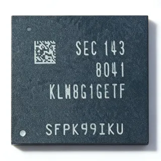
27C512-20 - 512Kbit EPROM 200ns CMOS 64Kx8 | Fujitsu
MPN: 27C512-20 ✗ End of Life| Qty | Unit Price | Extended |
|---|---|---|
| 1 | $6.5 | $6.50 |
| 10 | $5.85 | $58.50 |
| 100 | $5.2 | $520.00 |
| 500 | $4.68 | $2,340.00 |
| 1,000 | $4.1 | $4,100.00 |
Drop-in alternatives for 27C512-20 — same package, pin-to-pin compatible. Different-package parts requiring PCB rework are excluded.
Quick Comparison Tool — Select alternative parts for side-by-side comparison:
M27C512-20XF1
✅ Drop-In📋 Reference alternative (not in catalog)
AT27C512R-70PU
✅ Drop-In📋 Reference alternative (not in catalog)
TC57512AD
✅ Drop-In📋 Reference alternative (not in catalog)
M5M27C512AK
✅ Drop-In📋 Reference alternative (not in catalog)
W27C512-45
✅ Drop-In📋 Reference alternative (not in catalog)
GLS27SF512
✅ Drop-In📋 Reference alternative (not in catalog)
27C512-20/K
✅ Drop-In📋 Reference alternative (not in catalog)
27C512-20 Maximum Ratings & Electrical Characteristics
| Memory Type | UV EPROM |
| Technology | CMOS |
| Density | 512 Kbit (524,288 bits) |
| Organization | 64K x 8 |
| Maximum Access Time | 200 ns |
| Supply Voltage (VCC) | 5 V |
| Outputs | 3-state |
| Operation | Asynchronous |
| Package | CQCC32 / LCC32 (ceramic, UV window) |
| Mounting Type | Surface Mount |
| Erase Method | Ultraviolet light |
| Interface | Parallel |
| Word Size | 8 bit |
| Address Count | 65,536 words |
27C512-20 Pin Configuration
| Pin 1 | A15 — Address input bit 15 |
| Pin 2 | A12 — Address input bit 12 |
| Pin 3 | A7 — Address input bit 7 |
| Pin 4 | A6 — Address input bit 6 |
| Pin 5 | A5 — Address input bit 5 |
| Pin 6 | A4 — Address input bit 4 |
| Pin 7 | A3 — Address input bit 3 |
| Pin 8 | A2 — Address input bit 2 |
| Pin 9 | A1 — Address input bit 1 |
| Pin 10 | A0 — Address input bit 0 |
| Pin 11 | Q0 — Data output bit 0 (3-state) |
| Pin 12 | Q1 — Data output bit 1 (3-state) |
| Pin 13 | Q2 — Data output bit 2 (3-state) |
| Pin 14 | GND — Ground |
| Pin 15 | Q3 — Data output bit 3 (3-state) |
| Pin 16 | Q4 — Data output bit 4 (3-state) |
| Pin 17 | Q5 — Data output bit 5 (3-state) |
| Pin 18 | Q6 — Data output bit 6 (3-state) |
| Pin 19 | Q7 — Data output bit 7 (3-state) |
| Pin 20 | /E — Chip enable (active low) |
| Pin 21 | A10 — Address input bit 10 |
| Pin 22 | /OE/VPP — Output enable (active low) / programming voltage |
| Pin 23 | A11 — Address input bit 11 |
| Pin 24 | A9 — Address input bit 9 |
| Pin 25 | A8 — Address input bit 8 |
| Pin 26 | A13 — Address input bit 13 |
| Pin 27 | A14 — Address input bit 14 |
| Pin 28 | NC — Not connected (per JEDEC 27C512 PLCC32 layout) |
| Pin 29 | NC — Not connected |
| Pin 30 | NC — Not connected |
| Pin 31 | NC — Not connected |
| Pin 32 | VCC — Power supply, 5 V |
Safe Operating Area (SOA) & Thermal Characteristics
No official SOA curve available for this digital IC. Always operate within absolute maximum ratings specified in the datasheet. Ensure adequate cooling and derate as needed.
Typical Applications
27C512-20 is suitable for 6 applications: Legacy Embedded Controller Firmware, Arcade Game and Retro-Computing Cartridges, Industrial Equipment BIOS and Boot Code, Development and Prototype Firmware Storage, Telecom and Network Card Configuration Memory, Automotive and Test Equipment Firmware.
Legacy Embedded Controller Firmware
The 27C512-20 stores boot and application firmware in 8-bit microcontroller systems built around 5V buses, where its 64K x 8 organization maps directly to a full 64 KB code space and the 200 ns access time meets classic 5-8 MHz CPU timing without wait states. Plugged into the JEDEC 27C512 socket with /CE tied to address decode and /OE to the CPU read strobe, the device provides deterministic, unalterable code storage. The UV window allows field revision during development, and CMOS standby current keeps idle system power low. Modern maintenance of such systems typically uses faster EPROM or Flash substitutes, but original-grade silicon preserves authentic timing margins.
Recommended
Arcade Game and Retro-Computing Cartridges
Arcade PCBs and vintage home computers of the 1980s-90s use 27C512 sockets for game code and character ROMs. The 27C512-20's 64K x 8 capacity and 5V parallel interface match these boards exactly, and its ceramic LCC32 package suits surface-mounted or socketed cartridge positions. According to the eharmon EPROM cross-reference, hobbyists commonly mix original EPROMs with W27C512 EEPROM or GLS27SF512 Flash substitutes in these sockets for easier reprogramming during multi-game mod kits. When restoring to factory condition, the -20 grade's 200 ns speed matches original timing on 12 MHz-class 68000 and Z80 buses without introducing wait-state or bus-contention issues.
Recommended
Industrial Equipment BIOS and Boot Code
PLC controllers, CNC machines, medical devices, and telecom line cards of that era store BIOS, monitor, and diagnostic code in 27C512 sockets. The 27C512-20's non-volatile CMOS EPROM retains code through power cycles and decades of storage, with 3-state outputs permitting multiple memories on a shared 8-bit bus via /CE address decoding. Its 200 ns access time is conservative but adequate for the 4-8 MHz processor clocks typical of such equipment. Because the part is obsolete, service organizations qualifying replacements should verify M27C512 or AT27C512R pin-to-pin equivalence and confirm programming-voltage compatibility of their EPROM programmers before swapping devices.
Recommended
Development and Prototype Firmware Storage
The ceramic package's ultraviolet window makes the 27C512-20 suitable for iterative firmware development: code is erased with a UV lamp in minutes and reprogrammed, unlike OTP variants which are single-use. The JEDEC pinout lets the same target board accept development EPROMs and production OTP or Flash devices interchangeably. The 200 ns grade supports conventional microprocessor buses of legacy designs, while the single 5V read supply simplifies bench setups - only programming equipment needs the higher VPP. Engineers should verify their programmer supports the CMOS 27C512 algorithm, since NMOS-era algorithms can overstress CMOS dies during programming pulses.
Recommended
Telecom and Network Card Configuration Memory
Line cards, modems, and network interface boards from the late 1980s and 1990s use 27C512 devices for configuration tables, DSP boot code, and protocol firmware. The 27C512-20's 64K x 8 parallel organization, 5V-only read operation, and 3-state bus outputs integrate directly into these card designs, with the ceramic LCC32 providing a durable, socketed surface-mount option. The 200 ns access time comfortably serves the slower bus cycles of these subsystems. For telephony equipment still in service, replacement strategy matters: ST M27C512 and Microchip AT27C512R remain the lowest-risk drop-ins, while Flash substitutes enable field updates without desoldering.
Recommended
Automotive and Test Equipment Firmware
Engine control units, diagnostic testers, and bench instruments of the EPROM era hold calibration tables and firmware in 27C512 sockets. The 27C512-20's absolute non-volatility, 5V CMOS read interface, and wide availability during that period made it a default choice, and its 64K x 8 capacity matches the memory map window allocated in typical 8/16-bit controllers. The 200 ns access time suits the modest clock rates of these ECUs and testers. Tune shops modifying such ECUs today commonly install socketed EPROMs or Flash replacements (SST27SF512, W27C512) for repeatable reprogramming of calibration maps during iterative testing.
Recommended
Recommended Products Summary
Engineering reference data for 27C512-20 — comparison, design guidance, and compliance information.
Selection Guide
Comparison with Alternatives
| Parameter | This Product | M27C512-20XF1 | AT27C512R-70PU | W27C512-45 | GLS27SF512 |
|---|---|---|---|---|---|
| Package | CQCC32 / LCC32 (ceramic) | PLCC32 - same footprint | DIP28 / PLCC32 family | DIP28 / PLCC32 | DIP28 / PLCC32 |
| Brand | Fujitsu | STMicroelectronics | Microchip Technology | Winbond | Greenliant |
| Organization | 64K x 8 | 64K x 8 | 64K x 8 | 64K x 8 | 64K x 8 |
| Max Access Time | 200 ns | 200 ns | 70 ns (faster) | 45-120 ns (faster) | 70 ns (faster) |
| Supply Voltage | 5 V | 5 V | 5 V read | 5 V read | 5 V read |
| Erase Method | UV (ceramic window) | UV or OTP variant | OTP (PU) / UV window variants | Electrical (EEPROM) | Electrical (Flash) |
| Lifecycle Status | Obsolete | Active / mature | Active | Legacy / surplus | Active |
| In-System Reprogrammable | No (UV lamp required) | No (UV lamp required) | No (OTP/UV only) | Yes (electrical) | Yes (electrical/Flash) |
Key Differentiators
- Authentic Fujitsu silicon for restoration-grade repairs (vs M27C512-20XF1)
- UV-erasable ceramic window allows repeated reuse (vs AT27C512R-70PU)
- Slower 200 ns grade limits use on fast buses (vs W27C512-45)
Design Notes
Verify the programmer algorithm before programming. CMOS 27C512 devices require different VPP levels and pulse widths than NMOS 27xx EPROMs; using an NMOS algorithm can overstress the CMOS die. Confirm the exact suffix (-20, -20/L, -20/J, -20/K) package and speed options against the Fujitsu datasheet before creating a programming file, and never erase/program the original device in valuable vintage boards - program a known replacement instead, as recommended by EPROM repair guides.
When substituting a faster device (AT27C512R at 45-70 ns, W27C512 at 45 ns) into a board designed for the 200 ns 27C512-20, bus timing generally improves, but check output-enable and chip-enable access timing against the host CPU strobes. On boards with slow address decoding or wait-state logic tuned for 200 ns, faster devices are safe; the reverse substitution (slower in place of fast) requires wait states and is the usual failure mode.
The ceramic LCC32/PLCC32 footprint differs mechanically from DIP28: confirm your board uses the 32-pad PLCC/LCC land pattern with pin 1 at the notched corner matching the JEDEC orientation. For socketed retro-computing applications, use a quality machined-pin PLCC socket to avoid contact-resistance drift. Decouple VCC (pin 32) to GND (pin 14) with a 0.1 uF ceramic capacitor placed within a few millimeters of the package.
Compliance Information
Part predates RoHS/REACH (obsolete ceramic-package EPROM); no published compliance data found in provided sources.