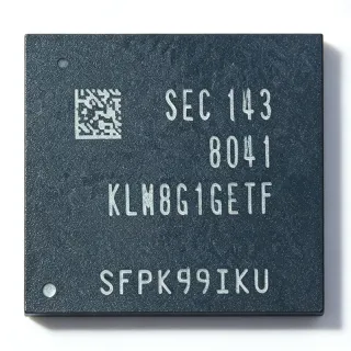
27C512L-15T - 512Kbit 64Kx8 CMOS EPROM 150ns | WSI
MPN: 27C512L-15T ✗ End of Life| Qty | Unit Price | Extended |
|---|---|---|
| 1 | $0 | $0.00 |
| 10 | $0 | $0.00 |
| 100 | $0 | $0.00 |
| 500 | $0 | $0.00 |
| 1,000 | $0 | $0.00 |
Drop-in alternatives for 27C512L-15T — same package, pin-to-pin compatible. Different-package parts requiring PCB rework are excluded.
Quick Comparison Tool — Select alternative parts for side-by-side comparison:
27C512-15FA
✅ Drop-In✓ In Stock
$1.65 / Unit
View Datasheet →27C512MC-15
✅ Drop-In✓ In Stock
$2.75 / Unit
View Datasheet →27C512QC-55
✅ Drop-In✓ In Stock
$4.22 / Unit
View Datasheet →27C512-20FA
✅ Drop-In✓ In Stock
$1.85 / Unit
View Datasheet →27C512-20
✅ Drop-In✓ In Stock
$4.1 / Unit
View Datasheet →27C512-25-X
✅ Drop-In✓ In Stock
$2.95 / Unit
View Datasheet →27C512-15/LP
✅ Drop-In📋 Reference alternative (not in catalog)
27C512-15FA
✅ Drop-In✓ In Stock
$1.65 / Unit
View Datasheet →27C512L-15T Maximum Ratings & Electrical Characteristics
| Memory Type | CMOS UV/OTP EPROM |
| Density | 512 Kilobit (64K x 8) |
| Organization | 64K x 8-bit |
| Access Time | 150 ns (-15 speed grade) |
| Supply Voltage | +5 V +/-10% |
| Programming Voltage (VPP) | +12.5 V |
| Programming Algorithm | 100% Flashrite programming |
| Standby Current (CMOS) | 20 uA typical |
| Interface | Parallel |
| Pinout Standard | JEDEC-approved 27C512 pinout |
| Package | 32-PLCC (T suffix) |
| Mounting Type | Surface Mount |
| Output Type | Tri-state, 8-bit data bus (O0-O7) |
| Address Inputs | A0-A15 (16 address lines) |
| Control Signals | CE, OE, VPP |
| RoHS Status | unknown |
27C512L-15T 32-plcc (t suffix) Pin Configuration Guide
Complete pinout information for 27C512L-15T (32-plcc (t suffix) package). This digital IC includes GPIO, communication interfaces (UART, SPI, I2C), and power pins. Refer to the manufacturer datasheet for alternate pin functions and configuration options. Essential for embedded system design and PCB layout.

No detailed pinout data available for 27C512L-15T.
Refer to the datasheet for full pin configuration.
Safe Operating Area (SOA) & Thermal Characteristics
No official SOA curve available for this digital IC. Always operate within absolute maximum ratings specified in the datasheet. Ensure adequate cooling and derate as needed.
Typical Applications
27C512L-15T is suitable for 6 applications: Legacy Firmware Storage in Industrial Controllers, Automotive ECU Repair and Remanufacturing, Telecom Line Card and Network Equipment Maintenance, Arcade, Pinball, and Coin-Op Game Restoration, Test and Measurement Instrument Firmware, BIOS and Embedded Board Firmware Replacement.
Legacy Firmware Storage in Industrial Controllers
The 27C512L-15T stores boot code and application firmware in PLCs, motor drives, and factory automation boards built around 8-bit MCUs. Its 64K x 8 organization maps directly onto 16-bit address buses (A0-A15), and the 150 ns access time supports CPU clocks of roughly 8-10 MHz without wait states. The single +5 V supply with +/-10% tolerance matches legacy industrial 5 V rails, and the JEDEC-approved pinout means a failed WSI part can be replaced by TI, ST, or Microchip 27C512 equivalents without PCB changes. The ~20 uA typical CMOS standby current limits drain in battery-backed controller memories. Performance consideration: reprogramming requires UV erasure or a fresh OTP device and a programmer supporting the 12.5 V Flashrite algorithm.
Recommended
Automotive ECU Repair and Remanufacturing
Engine control units and body controllers from the 1980s-1990s frequently use 27C512 EPROMs for calibration tables and firmware. The 27C512L-15T offers a drop-in repair path: its JEDEC pinout and 64K x 8 organization match the original socket, and the -15 grade meets typical ECU bus timing. Because the L-grade draws only ~20 uA typical CMOS standby current, keep-alive memory rails are minimally loaded. Service shops re-burn updated fuel/spark maps into a blank OTP 27C512 and replace the socketed device. Note that automotive under-hood environments require the correct temperature-grade suffix; verify the commercial vs industrial variant against the original BOM before substitution.
Recommended
Telecom Line Card and Network Equipment Maintenance
Legacy telecom rack equipment - channel banks, modems, and PBX cards - stores monitor code in 27C512 sockets. The 27C512L-15T suits spares programs: its parallel interface (CE, OE, tri-state data outputs) is trivially compatible with legacy bus architectures, and the 150 ns access time covers typical line-card processor timing. Stocking one 27C512 footprint spare covers multiple vendors' boards thanks to the JEDEC-standard pinout shared by TI TMS27C512, ST 27C512, and Intel CHMOS 27C512. Consideration: OTP versions cannot be erased for re-use; windowed ceramic packages (UV-erasable) are preferable where repeated re-programming of a spare is needed.
Recommended
Arcade, Pinball, and Coin-Op Game Restoration
The coin-op restoration community relies on 27C512 EPROMs to rebuild game ROM sets, and the 27C512L-15T is a direct fit for boards designed for the 27C512 footprint. The 64K x 8 organization holds character/tile ROMs or program code segments, and the JEDEC pinout allows any vendor's 27C512 of equal or faster speed to be burned with the original image. The 150 ns -15 grade safely replaces slower original parts, but substituting a slower -20 or -25 grade into a timing-critical arcade board can cause graphical corruption or crashes, so match or exceed speed. Verify VPP requirements (12.5 V) against your EPROM programmer's algorithm list.
Recommended
Test and Measurement Instrument Firmware
Older oscilloscopes, spectrum analyzers, and logic analyzers store boot firmware and calibration constants in 27C512 devices. The 27C512L-15T supports these sockets with its 64K x 8 array and 150 ns access time; its +/-10% supply tolerance tolerates noisy instrument power rails. For cal-lab environments, the CMOS low standby current (~20 uA typical) helps battery-powered portable instruments. Replacement workflow: read the original device, verify the checksum, program a fresh OTP 27C512, and re-seat. Because many instruments checksum their ROM at power-up, a partially programmed or marginal device will fail POST - always verify programmed content on the programmer before field installation.
Recommended
BIOS and Embedded Board Firmware Replacement
PC motherboards, single-board computers, and embedded controllers of the 286/386 era used 27C512 EPROMs for system BIOS. The 27C512L-15T's 150 ns access time meets ISA-era BIOS fetch timing, and its 64K x 8 capacity matches the classic 64 KB BIOS image size. Repair technicians burn a known-good BIOS dump into a replacement device, preserving the original DIP-28/PLCC-32 footprint. The JEDEC-standard pinout means ST, TI, Intel, and Philips 27C512 parts are interchangeable in the same socket. Consideration: check whether the board decodes A15 - some boards treat the 27C512 as two banked 32 KB images selected by a jumper.
Recommended
Recommended Products Summary
Engineering reference data for 27C512L-15T — comparison, design guidance, and compliance information.
Selection Guide
Comparison with Alternatives
| Parameter | This Product | 27C512-15FA | 27C512-15/LP | 27C512-15 |
|---|---|---|---|---|
| Package | 32-PLCC | 32-PLCC - same | 32-PLCC - same | PLCC/DIP variants - verify footprint |
| Brand | WaferScale Integration (WSI) | WaferScale Integration | Microchip Technology | STMicroelectronics |
| Density / Organization | 512 Kbit, 64K x 8 | 512 Kbit, 64K x 8 | 512 Kbit, 64K x 8 | 512 Kbit, 64K x 8 |
| Access Time | 150 ns | 150 ns | 150 ns | 150 ns |
| Supply Voltage | +5 V +/-10% | +5 V +/-10% | +5 V | +5 V |
| Programming Voltage (VPP) | +12.5 V | +12.5 V | +12.5 V | +12.5 V |
| Standby Current | 20 uA typical (CMOS, L grade) | [DATA_NEEDED] | [DATA_NEEDED] | [DATA_NEEDED] |
| Pinout Standard | JEDEC-approved 27C512 | JEDEC 27C512 - identical | JEDEC 27C512 - identical | JEDEC 27C512 - identical |
| Lifecycle Status | Obsolete | Obsolete (aftermarket) | Aftermarket via Rochester | Obsolete (aftermarket) |
Key Differentiators
- Low-power L-grade CMOS standby (vs 27C512-20)
- Faster timing headroom available in same family (vs 27C512-25-X)
- JEDEC-approved pinout enables cross-vendor sourcing (vs 27C512-15/LP)
Design Notes
The 27C512L-15T operates from a single +5 V supply with a standard +/-10% tolerance (4.5 V to 5.5 V). Decouple VCC with a 0.1 uF ceramic capacitor placed within 10 mm of the device, shared per socket on legacy boards. The L-grade CMOS design draws roughly 20 uA typical standby current when CE is high, so battery-backed rail designs see negligible drain; active read current should be budgeted from the datasheet ICC specification for your speed grade before sizing the 5 V rail.
Speed-grade substitution is the most common failure mode: replacing a -15 part with a -20 or -25 grade in a socket designed for 150 ns timing causes intermittent data corruption that often appears only at temperature extremes. Always match or exceed the original speed grade. Also confirm the package: 32-PLCC and 28-DIP versions of the 27C512 share the JEDEC pinout but are not mechanically interchangeable; adapters exist but add reliability risk in vibrating environments.
Tie unused control inputs to defined levels: CE and OE must be actively driven, never left floating, or the tri-state outputs may float and cause bus contention. Keep address/data trace lengths roughly matched on bus-heavy boards to minimize skew; for 150 ns timing budgets, skew of a few ns is tolerable but cumulative trace stubs on PLCC-to-DIP adapters can erode margin. Verify VPP is connected to +12.5 V only during programming - in normal read operation VPP/VCC pin must sit at VCC per the JEDEC 27C512 pinout.
Compliance Information
Device is obsolete; the original WSI 27C512L-15T predates modern RoHS enforcement and may contain lead in lead-frame finish and UV-window solder. No compliance data was found in the verified web sources.