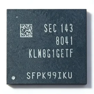
27C512-20FA - 512Kbit 64Kx8 UV/OTP EPROM 200ns | NXP
MPN: 27C512-20FA ✗ End of Life| Qty | Unit Price | Extended |
|---|---|---|
| 1 | $3.2 | $3.20 |
| 10 | $2.9 | $29.00 |
| 100 | $2.55 | $255.00 |
| 500 | $2.2 | $1,100.00 |
| 1,000 | $1.85 | $1,850.00 |
Drop-in alternatives for 27C512-20FA — same package, pin-to-pin compatible. Different-package parts requiring PCB rework are excluded.
Quick Comparison Tool — Select alternative parts for side-by-side comparison:
27C512-15FA
✅ Drop-In✓ In Stock
$1.65 / Unit
View Datasheet →27C512-20
✅ Drop-In ⚠️ 参数待验证✓ In Stock
$4.1 / Unit
View Datasheet →27C512-25-X
✅ Drop-In✓ In Stock
$2.95 / Unit
View Datasheet →27C512MC-15
✅ Drop-In✓ In Stock
$2.75 / Unit
View Datasheet →27C512QC-55
✅ Drop-In ⚠️ 参数待验证✓ In Stock
$4.22 / Unit
View Datasheet →M27C512-12F1
✅ Drop-In📋 Reference alternative (not in catalog)
AT27C512R-70PU
✅ Drop-In📋 Reference alternative (not in catalog)
27C512-20FA Maximum Ratings & Electrical Characteristics
| Memory Size | 524,288 bit (512 Kbit) |
| Organization | 64K x 8 |
| Maximum Access Time | 200 ns |
| Supply Voltage Range | 4.5 V to 5.5 V |
| Technology | CMOS EPROM |
| Memory Type | UV / OTP EPROM (non-volatile) |
| Temperature Grade | Commercial |
| Number of Terminals | 28 |
| Package Code | DIP (rectangular) |
| Mounting Type | Through Hole |
| Access Mode | Asynchronous |
| Output Type | Tri-state, 8-bit parallel |
| Address Inputs | A0 to A15 (16-bit address bus) |
| Control Signals | /CE (chip enable), /OE (output enable), /PGM |
| RoHS Status | unknown |
| Operating Supply Nominal | 5 V |
27C512-20FA Pin Configuration
| Pin 1 | A15 — Address input bit 15 |
| Pin 2 | A12 — Address input bit 12 |
| Pin 3 | A7 — Address input bit 7 |
| Pin 4 | A6 — Address input bit 6 |
| Pin 5 | A5 — Address input bit 5 |
| Pin 6 | A4 — Address input bit 4 |
| Pin 7 | A3 — Address input bit 3 |
| Pin 8 | A2 — Address input bit 2 |
| Pin 9 | A1 — Address input bit 1 |
| Pin 10 | A0 — Address input bit 0 |
| Pin 11 | D0 — Data output bit 0 (tri-state) |
| Pin 12 | D1 — Data output bit 1 (tri-state) |
| Pin 13 | D2 — Data output bit 2 (tri-state) |
| Pin 14 | GND — Ground |
| Pin 15 | D3 — Data output bit 3 (tri-state) |
| Pin 16 | D4 — Data output bit 4 (tri-state) |
| Pin 17 | D5 — Data output bit 5 (tri-state) |
| Pin 18 | D6 — Data output bit 6 (tri-state) |
| Pin 19 | D7 — Data output bit 7 (tri-state) |
| Pin 20 | /CE — Chip enable (active low); also /PGM during programming |
| Pin 21 | A10 — Address input bit 10 |
| Pin 22 | /OE — Output enable (active low) / VPP during programming |
| Pin 23 | A11 — Address input bit 11 |
| Pin 24 | A9 — Address input bit 9 |
| Pin 25 | A8 — Address input bit 8 |
| Pin 26 | A13 — Address input bit 13 |
| Pin 27 | A14 — Address input bit 14 |
| Pin 28 | VCC — Power supply, 4.5 V to 5.5 V |
Safe Operating Area (SOA) & Thermal Characteristics
No official SOA curve available for this digital IC. Always operate within absolute maximum ratings specified in the datasheet. Ensure adequate cooling and derate as needed.
Typical Applications
27C512-20FA is suitable for 6 applications: Retrocomputer and Arcade Board Restoration, Legacy Embedded Controller Firmware Storage, Mask ROM Prototyping and Emulation, Automotive and Machinery Diagnostic Cartridges, Character Generators and Lookup Tables in Test Instruments, Coin-Operated and Slot Machine Firmware.
Retrocomputer and Arcade Board Restoration
The 27C512-20FA is a primary choice for restoring vintage 8-bit and 16-bit computers, arcade PCBs, and game consoles that were designed around the industry-standard 27C512 EPROM socket. Its 64K x 8 organization and 200 ns access time match the bus timing of Z80, 6502, 6809, and 68000-based boards from the 1980s and 1990s. Programmers dump the original ROM image with an EPROM reader, then burn it onto the 27C512-20FA for a functionally identical replacement. Because it is a CMOS part, power consumption stays low, which matters in battery-backed or thermally enclosed cabinets. For boards needing repeated firmware iteration, windowed variants or Flash-emulating substitutes can be interleaved during development, with the 27C512-20FA installed as the final production-authentic device.
Recommended
Legacy Embedded Controller Firmware Storage
Industrial controllers, motor drives, test equipment, and telecommunications boards designed in the 1990s often store boot firmware and lookup tables in a 27C512 socket. The 27C512-20FA provides non-volatile storage that requires no configuration: the host CPU simply asserts /CE and /OE, waits up to 200 ns, and reads data. Its 4.5V to 5.5V CMOS operation interfaces directly with 5V microprocessors and ASICs without level translation. When an OEM end-of-lifes the original mask ROM order, engineering teams use the 27C512-20FA as a field-service replacement, programming the validated firmware image onto each device. Its commercial temperature grade covers the 0C to +70C range typical of indoor industrial environments, keeping service inventory simple.
Recommended
Mask ROM Prototyping and Emulation
Before committing to a mask ROM for volume production, engineers prototype firmware in EPROMs because they can be reprogrammed in-house with an EPROM programmer. The 27C512-20FA emulates a 64KB mask ROM electrically: same asynchronous read interface, same tri-state outputs, same /CE and /OE timing. Once the firmware is frozen, the design moves to a masked ROM or Flash device for volume. During prototyping, the 200 ns access time gives comfortable timing margin on typical 8-bit buses running up to roughly 8 MHz. The DIP-28 through-hole package also supports zero-insertion-force sockets, letting engineers swap firmware images in seconds during iterative debugging without soldering rework.
Recommended
Automotive and Machinery Diagnostic Cartridges
Service diagnostics and tuning modules for older vehicles and heavy machinery frequently use 27C512 EPROMs in replaceable cartridges, including engine management reference maps and dealer diagnostic software. The 27C512-20FA fits these sockets directly, storing up to 64KB of calibration or diagnostic code readable by the onboard 5V ECU. Its CMOS construction tolerates the modest supply fluctuation of vehicle electrical systems within the 4.5V to 5.5V window when the carrier board includes regulation. Technicians program updated maps onto fresh devices and swap the cartridge, avoiding in-system flashing complexity. For applications subjected to under-hood temperatures, verify the commercial grade is sufficient, or seek an industrial-temperature speed-grade equivalent of the same family.
Recommended
Character Generators and Lookup Tables in Test Instruments
Bench instruments, CRT character generators, barcode readers, and protocol analyzers of the pre-Flash era stored font bitmaps, state tables, and calibration constants in 27C512 EPROMs. The parallel asynchronous interface of the 27C512-20FA lets address counters or microcontrollers stream table entries with deterministic 200 ns latency - an advantage over serial Flash whose random-access timing is harder to bound in glitch-sensitive display scan chains. The 64KB density covers typical 8x16 font sets for full ASCII and extended character pages with room to spare. Designers wiring new scan hardware today still replicate this pattern for deterministic ROM streaming using the same DIP-28 footprint, making this part valuable for both service and reproduction of legacy instruments.
Recommended
Coin-Operated and Slot Machine Firmware
Gaming, vending, and amusement machines from the 1990s store prize logic, RNG tables, and regulatory-certified firmware in soldered or socketed 27C512 EPROMs, because regulators require that certified code not be field-modifiable - a property OTP and UV EPROMs satisfy inherently. The 27C512-20FA is used to replace failed or tampered ROMs with freshly programmed, audit-approved images. Its one-time or UV-only erasure provides tamper evidence: any modification requires physically replacing the device, which supports compliance audits. The commercial grade suits the climate-controlled indoor environment of these machines, and the DIP-28 package matches original sockets, letting certified service centers perform board-level swaps without redesigning the host PCB.
Recommended
Recommended Products Summary
Engineering reference data for 27C512-20FA — comparison, design guidance, and compliance information.
Selection Guide
Comparison with Alternatives
| Parameter | This Product | 27C512-15FA | 27C512-25-X | 27C512QC-55 | M27C512-12F1 | AT27C512R-70PU |
|---|---|---|---|---|---|---|
| Package | DIP-28 | DIP-28 - same | DIP-28 - same | PLCC-32 - different package, same die | DIP-28 - same | DIP-28 - same |
| Brand | NXP Semiconductors (Signetics) | NXP Semiconductors | NXP Semiconductors | NXP Semiconductors | STMicroelectronics | Microchip Technology |
| Maximum Access Time | 200 ns | 150 ns | 250 ns | 55 ns | 120 ns | 70 ns |
| Organization | 64K x 8 (512 Kbit) | 64K x 8 | 64K x 8 | 64K x 8 | 64K x 8 | 64K x 8 |
| Supply Voltage | 4.5 V to 5.5 V | 4.5 V to 5.5 V | 4.5 V to 5.5 V | 4.5 V to 5.5 V | 4.5 V to 5.5 V | 4.5 V to 5.5 V |
| Memory Technology | CMOS UV/OTP EPROM | CMOS UV/OTP EPROM | CMOS UV/OTP EPROM | CMOS EPROM | CMOS UV/OTP EPROM | OTP Flash-emulated EPROM |
| Temperature Grade | Commercial | [DATA_NEEDED] | [DATA_NEEDED] | [DATA_NEEDED] | [DATA_NEEDED] | [DATA_NEEDED] |
| Unit Price (qty 1, as of 2026-09-13) | $3.20 | [DATA_NEEDED] | [DATA_NEEDED] | [DATA_NEEDED] | [DATA_NEEDED] | [DATA_NEEDED] |
Key Differentiators
- 200 ns speed grade balances cost and compatibility (vs 27C512-15FA)
- Guaranteed fit in original Signetics-designed sockets (vs M27C512-12F1)
- Availability of faster cross-brand drop-ins (vs AT27C512R-70PU)
Design Notes
Verify bus timing margin before selecting the 200 ns grade. For a Z80 at 8 MHz, a memory cycle allows roughly 250 ns from address valid to data sampled, so the 27C512-20FA fits with margin after address-decode delays. For 16 MHz 68000 designs, use a 150 ns or faster grade such as the 27C512-15FA. Estimated: a 68000 at 16 MHz provides about 220 ns of ROM access time per 4-cycle read, leaving less than 20 ns for glue-logic decode - too tight for a 200 ns part.
Do not confuse UV-windowed and OTP variants: the OTP plastic DIP cannot be erased, and programming failures cannot be recovered by re-burning. Distributor records for the 27C512-20FA (Vyrian: OTP ROM) suggest this suffix is OTP, so order exactly the number of devices needed plus spares. Also note pin 20 is /CE on read and /PGM during programming - programmers that use /CE-based algorithms must not be used with /OE-timed programming setups without verifying the datasheet programming algorithm.
Use a quality machine-tooled or dual-wipe socket rather than soldering DIP-28 EPROMs directly when field replacement or firmware updates are expected. Keep VCC/GND decoupling (0.1 uF ceramic) within 10 mm of pin 28/pin 14 to suppress read-current transients. For UV-windowed ceramic variants in electrically noisy environments, cover the window with an opaque label - ambient fluorescent light can slowly degrade cell charge over years of service.
The 27C512-20FA is a CMOS EPROM operating at 4.5V to 5.5V; it must not be connected to 3.3V buses without level shifting. Standby current is low in CMOS mode (device deselected via /CE high), so battery-backed designs should gate /CE rather than /OE to obtain the lowest standby consumption. Estimated: at typical CMOS EPROM standby levels of a few hundred microamps, a 2000 mAh backup cell supports multi-year retention of board power-up state.
Compliance Information
Obsolete part predating RoHS-era compliance records; distributor listings do not state RoHS status. Many 27C512 devices were manufactured with leaded through-hole finishes - assume non-RoHS unless the specific date code is verified.