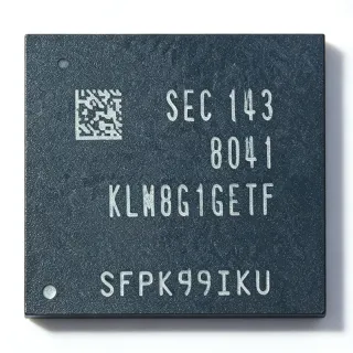
27C512-25-X - 512Kbit 64Kx8 UV EPROM 250ns | Fujitsu
MPN: 27C512-25-X ✗ End of Life| Qty | Unit Price | Extended |
|---|---|---|
| 1 | $4.95 | $4.95 |
| 10 | $4.45 | $44.50 |
| 100 | $3.95 | $395.00 |
| 500 | $3.45 | $1,725.00 |
| 1,000 | $2.95 | $2,950.00 |
Drop-in alternatives for 27C512-25-X — same package, pin-to-pin compatible. Different-package parts requiring PCB rework are excluded.
Quick Comparison Tool — Select alternative parts for side-by-side comparison:
27C512-20
✅ Drop-In✓ In Stock
$4.1 / Unit
View Datasheet →27C512-15FA
✅ Drop-In✓ In Stock
$1.65 / Unit
View Datasheet →27C512A-12I/SO
✅ Drop-In✓ In Stock
$2.85 / Unit
View Datasheet →W27C512
✅ Drop-In📋 Reference alternative (not in catalog)
M27C512
✅ Drop-In📋 Reference alternative (not in catalog)
AT27C512R
✅ Drop-In📋 Reference alternative (not in catalog)
TMS27C512
✅ Drop-In📋 Reference alternative (not in catalog)
27C512-25-X Maximum Ratings & Electrical Characteristics
| Memory Size | 512 Kbit (64K x 8) |
| Organization | 65,536 words x 8 bits |
| Memory Type | UV EPROM |
| Access Time | 250 ns |
| Supply Voltage (Read) | 5 V +/- 10% |
| Technology | CMOS |
| Interface | Parallel |
| Address Lines | 15 (A0-A14) |
| Data Lines | 8 (D0-D7), 3-state outputs |
| Control Signals | /CE (chip enable), /OE (output enable), /PGM (program) |
| Package | 28-pin DIP (windowed ceramic or plastic OTP variant per suffix) |
| Mounting Type | Through Hole |
| Pinout | JEDEC-approved 27C512 pinout |
| RoHS Status | unknown (legacy non-RoHS-era part) |
27C512-25-X Pin Configuration
| Pin 1 | A15 — Address line 15 (highest-order address bit) |
| Pin 2 | A12 — Address line 12 |
| Pin 3 | A7 — Address line 7 |
| Pin 4 | A6 — Address line 6 |
| Pin 5 | A5 — Address line 5 |
| Pin 6 | A4 — Address line 4 |
| Pin 7 | A3 — Address line 3 |
| Pin 8 | A2 — Address line 2 |
| Pin 9 | A1 — Address line 1 |
| Pin 10 | A0 — Address line 0 (lowest-order address bit) |
| Pin 11 | D0 — Data output 0 (3-state) |
| Pin 12 | D1 — Data output 1 (3-state) |
| Pin 13 | D2 — Data output 2 (3-state) |
| Pin 14 | GND — Ground reference |
| Pin 15 | D3 — Data output 3 (3-state) |
| Pin 16 | D4 — Data output 4 (3-state) |
| Pin 17 | D5 — Data output 5 (3-state) |
| Pin 18 | D6 — Data output 6 (3-state) |
| Pin 19 | D7 — Data output 7 (3-state, MSB) |
| Pin 20 | /CE — Chip enable (active low); device select and standby control |
| Pin 21 | A10 — Address line 10 |
| Pin 22 | /OE — Output enable (active low); gates data outputs |
| Pin 23 | A11 — Address line 11 |
| Pin 24 | A9 — Address line 9; also VPP input in program mode on some variants |
| Pin 25 | A8 — Address line 8 |
| Pin 26 | A13 — Address line 13 |
| Pin 27 | A14 — Address line 14 |
| Pin 28 | VCC — +5 V power supply |
Safe Operating Area (SOA) & Thermal Characteristics
No official SOA curve available for this digital IC. Always operate within absolute maximum ratings specified in the datasheet. Ensure adequate cooling and derate as needed.
Typical Applications
27C512-25-X is suitable for 6 applications: Legacy Industrial Controller Firmware Storage, Retro Computing and Arcade Board Restoration, Automotive ECU and Engine Management Repair, Telecom Line Card and Network Equipment Maintenance, Test and Measurement Instrument Firmware, Embedded Systems Education and Prototyping.
Legacy Industrial Controller Firmware Storage
The 27C512-25-X stores boot and application firmware in PLCs, motor drives, and process controllers designed in the late 1980s through 1990s. Its 64K x 8 organization matches the 16-bit address space of popular 8-bit CPUs (Z80, 8051, 68HC11), and the 250 ns access time is adequate for clock rates up to roughly 8-12 MHz without wait states. The device's non-volatile storage retains program code during power loss, while the UV-erase capability permits field firmware updates by swapping pre-programmed devices. For sustaining these systems, JEDEC-pinout substitutes like W27C512 or M27C512 allow repair without PCB redesign.
Recommended
Retro Computing and Arcade Board Restoration
Vintage computers, game consoles, and arcade PCBs rely on 27C512 EPROMs for game code and character ROMs. The 27C512-25-X's JEDEC 28-pin pinout and 5 V single-supply operation make it directly interchangeable with original Fujitsu, TI, or NEC devices in these boards. Restorers typically program new 27C512-type devices with verified ROM dumps; the 250 ns grade meets the timing of original mid-1980s processors (68000 systems at 8-12 MHz typically require 200-350 ns ROMs). EEPROM-type W27C512 is favored because it allows iterative reprogramming without a UV eraser lamp and 20-minute erase cycles.
Recommended
Automotive ECU and Engine Management Repair
Many 1980s-1990s engine control units used a 27C512-class EPROM for fuel and ignition maps in a socketed DIP-28 position, allowing tuners and repair shops to reflash calibration data. The 27C512-25-X in a windowed ceramic package can be erased and reprogrammed for revised maps; its 250 ns access suits 8-bit ECUs (e.g., 68HC11-based systems). Note that automotive under-hood temperatures demand verification of the device's operating range, and vibration-prone sockets should be secured. EEPROM-type substitutes (W27C512) are popular because tuning iterations are faster without UV erase.
Recommended
Telecom Line Card and Network Equipment Maintenance
Telecom rack equipment (channel banks, multiplexers, PBX cards) from the 1990s stored configuration and protocol firmware in 27C512 sockets. The 27C512-25-X's 5 V +/- 10% tolerance supports noisy backplane supplies common in telecom racks, and CMOS standby current minimizes rack-level power draw across hundreds of memory devices. Field service organizations maintain 27C512 stock to repair these long-lived systems; because access time requirements are modest, faster JEDEC-pinout equivalents can substitute freely. Socketed placement enables simple firmware revision swaps during maintenance windows.
Recommended
Test and Measurement Instrument Firmware
Oscilloscopes, multimeters, and logic analyzers from the EPROM era stored self-test routines, calibration constants, and UI firmware in 27C512 devices. The 27C512-25-X provides 64 KB of code space, sufficient for compact instrument firmware, and its three-state data outputs share a CPU bus cleanly under /CE and /OE control. Repair technicians replacing failed EPROMs must preserve the exact firmware image; EEPROM-type drop-ins simplify the process. The 250 ns grade matches the moderate bus speeds of these instruments, and the device's non-volatility preserves calibration data through power cycles.
Recommended
Embedded Systems Education and Prototyping
The 27C512 family remains valuable in university labs teaching microprocessor interfacing because its simple parallel interface (15 address lines, 8 data lines, /CE, /OE) transparently demonstrates memory bus timing, address decoding, and wait-state analysis. The 27C512-25-X's 250 ns timing allows students to compute and observe access-time margins directly on an oscilloscope. UV-erase workflow teaches non-volatile memory fundamentals before introducing Flash.socketed DIP-28 placement on breadboard-to-DIP adapters supports rapid experiments. Modern equivalents (AT27C512R OTP) reduce cost for student volume kits.
Recommended
Recommended Products Summary
Engineering reference data for 27C512-25-X — comparison, design guidance, and compliance information.
Selection Guide
Comparison with Alternatives
| Parameter | This Product | 27C512-20 | 27C512-15FA | W27C512 | M27C512 | AT27C512R | TMS27C512 | 27C512A-12I/SO |
|---|---|---|---|---|---|---|---|---|
| Package | DIP-28 | DIP-28 - same | DIP-28 - same | DIP-28 - same | DIP-28 - same | DIP-28 - same | DIP-28 - same | SOIC-28 (SMD footprint) |
| Brand | Fujitsu | Fujitsu | Fujitsu | Winbond | STMicroelectronics | Microchip Technology | Texas Instruments | Microchip Technology |
| Access Time | 250 ns | 200 ns | 150 ns | 45-120 ns | 100-200 ns | 45-90 ns | 100-200 ns | 120 ns |
| Organization | 64K x 8 | 64K x 8 | 64K x 8 | 64K x 8 | 64K x 8 | 64K x 8 | 64K x 8 | 64K x 8 |
| Erase Type | UV erase (windowed) / OTP per suffix | UV erase | UV erase | Electrical erase (EEPROM) | UV or OTP ranges | OTP only | UV erase | OTP |
| Supply Voltage | 5 V +/- 10% | 5 V +/- 10% | 5 V +/- 10% | 5 V | 5 V +/- 10% | 5 V +/- 10% | 5 V +/- 10% | 5 V +/- 10% |
| Lifecycle Status | Obsolete | Obsolete (legacy stock) | Obsolete (legacy stock) | Active/legacy production (Winbond) | Active (ST legacy line) | Active (Microchip) | Obsolete (legacy stock) | Active (Microchip) |
| Pinout Standard | JEDEC 27C512, 28-pin | JEDEC 27C512 - same | JEDEC 27C512 - same | JEDEC 27C512 - same | JEDEC 27C512 - same | JEDEC 27C512 - same | JEDEC 27C512 - same | JEDEC 27C512 (SOIC-28) |
Key Differentiators
- UV-erase reusability (vs AT27C512R)
- Cost of obsolescence trade-off (vs W27C512)
- Speed grade selection flexibility (vs 27C512-20)
Design Notes
Verify CPU timing margin against the 250 ns access time: total delay includes address setup, CE/OE access, and output float times plus bus capacitance derating (add roughly 5-10 ns per 100 pF of bus load). For CPUs above about 8 MHz at temperature extremes, prefer a 150-200 ns grade (27C512-15FA/27C512-20) or a modern 45-90 ns AT27C512R. Consult the CPU datasheet's memory read cycle timing rather than assuming the nominal access time applies at worst-case conditions.
Confirm technology type before programming: UV EPROMs (this device, M27C512, TMS27C512) require VPP and a UV eraser; the Winbond W27C512 is electrically erasable and uses a different programming algorithm. Using the wrong algorithm in an EPROM programmer can damage the device. Also distinguish windowed ceramic DIP from plastic OTP packages - a plastic package has no window and cannot be erased, despite sharing the same pinout and part family.
For socketed legacy repairs, use a low-profile machined-pin DIP-28 socket to ensure reliable contact over decades of service, and label the socketed firmware version on the board. Add 100 nF decoupling directly across VCC (pin 28) and GND (pin 14). Tie /CE and /OE appropriately: grounding /OE and decoding /CE gives fastest access; grounding /CE only increases standby power but is acceptable in single-memory systems.
Compliance Information
Legacy pre-RoHS-era EPROM; Fujitsu no longer provides compliance declarations for this obsolete part. Verify with the distributing supplier for your specific stock lot.