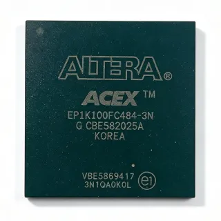
A54SX72A-1FG484I - 72K Gate Antifuse FPGA 250MHz | Microchip
MPN: A54SX72A-1FG484I ✓ Active| Qty | Unit Price | Extended |
|---|---|---|
| 1 | $258.31 | $258.31 |
| 10 | $245.4 | $2,454.00 |
| 100 | $231.2 | $23,120.00 |
| 500 | $219.6 | $109,800.00 |
| 1,000 | $208.5 | $208,500.00 |
A54SX72A-1FG484I Overview
An antifuse FPGA is a type of field-programmable gate array whose interconnects are permanently configured at power-up by blowing programmable antifuse links. Unlike SRAM-based FPGAs, antifuse devices are non-volatile, require no external configuration memory, and are inherently resistant to configuration bitstream readback attacks, which places them in the one-time-programmable (OTP) programmable logic category alongside CPLDs and flash-based FPGAs.
Key features of the A54SX72A include a 0.25um/0.22um CMOS process, low static power consumption typical of 2.5V antifuse architectures, dedicated global and quadrant clock networks (CLKA, CLKB, and QCLK) for low-skew clock distribution, and a sea-of-modules routing fabric that provides high gate utilization. The 360 available I/Os support a wide range of interface standards at 2.5V logic levels.
Architecturally, the SX-A family combines C-cell combinational logic modules with R-cell sequential modules, enabling efficient implementation of both wide combinational functions and registered pipelines. The antifuse interconnect provides deterministic, low-capacitance routing that supports the family's 250 MHz performance rating while keeping power draw low compared to SRAM FPGA alternatives.
Typical applications include industrial control and automation, secure military and aerospace logic integration, telecommunications line-card glue logic, and single-chip integration of multiple ASIC/SSI/MSI functions where configuration readback protection and instant-on operation matter.
A key design consideration: antifuse devices are one-time programmable, so prototype thoroughly in simulation and verify pinout assignments before programming; there is no rework path after programming errors.
This page synthesizes distributor pricing, drop-in same-family alternatives, and practical design notes not found in the manufacturer datasheet.
Drop-in alternatives for A54SX72A-1FG484I — same package, pin-to-pin compatible. Different-package parts requiring PCB rework are excluded.
Variants in this series
Same-series models that are drop-in compatible with A54SX72A-1FG484I (same form factor and footprint) — differing in RoHS Status, System Gates, Package, Operating Temperature, Process Technology.
Quick Comparison Tool — Select alternative parts for side-by-side comparison:
A54SX72A-1FGG484I
✅ Drop-In✓ In Stock
$225 / Unit
View Datasheet →A54SX72A-2FGG484I
✅ Drop-In✓ In Stock
$112 / Unit
View Datasheet →A54SX72A-FGG484I
✅ Drop-In✓ In Stock
$115 / Unit
View Datasheet →A54SX72A-1FGG484M
✅ Drop-In✓ In Stock
$73.4 / Unit
View Datasheet →A54SX72A-FFGG484
✅ Drop-In✓ In Stock
Contact for price
View Datasheet →A54SX72A-FGG484A
✅ Drop-In✓ In Stock
Contact for price
View Datasheet →A54SX72A-1FG484I Maximum Ratings & Electrical Characteristics
| Family | SX-A (Antifuse FPGA) |
| System Gates | 72,000 |
| Logic Cells (Modules) | 4,024 |
| Maximum System Frequency | 250 MHz |
| Process Technology | 0.25um/0.22um CMOS |
| Core Supply Voltage | 2.5 V |
| User I/O | 360 |
| Speed Grade | -1 |
| Programming Technology | Antifuse (one-time programmable) |
| Package | 484-ball FBGA |
| Mounting Type | Surface Mount |
| Operating Temperature | -40C to +85C (Industrial) |
| Temperature Grade Code | I (Industrial) |
| Packaging | Tray |
| Clock Networks | CLKA, CLKB, QCLK (global and quadrant) |
A54SX72A-1FG484I 484-ball fbga Pin Configuration Guide
Pin configuration for A54SX72A-1FG484I (484-ball fbga package). This digital IC includes GPIO, communication interfaces (UART, SPI, I2C), and power pins. Refer to the manufacturer datasheet for alternate pin functions and configuration options. Essential for embedded system design and PCB layout.

No detailed pinout data available for A54SX72A-1FG484I.
Refer to the datasheet for full pin configuration.
Typical Applications
A54SX72A-1FG484I is suitable for 6 applications: Industrial Control and Automation, Secure Defense and Aerospace Logic, Telecommunications Line-Card Glue Logic, Single-Chip ASIC/SSI/MSI Integration, Test and Measurement Instrumentation, Legacy Sustaining and Obsolescence Bridging.
Industrial Control and Automation
The A54SX72A-1FG484I fits industrial control and automation systems that need deterministic, instant-on logic without a configuration controller. Its industrial -40C to +85C rating, 2.5V low-power antifuse fabric, and 360 user I/Os allow integration of PLC I/O decoding, encoder interfaces, and interlock logic into a single 484-ball FBGA device. Because the antifuse configuration is non-volatile, machinery begins operating the moment power is applied, eliminating boot delay and configuration-corruption failure modes common to SRAM FPGAs. Designers should budget the -1 speed grade (250 MHz family maximum) with static timing margin in Libero, since antifuse programming cannot be revised after deployment.
Recommended
Secure Defense and Aerospace Logic
Antifuse FPGAs are a mainstay in defense and aerospace electronics because the programmed interconnect offers no readable configuration bitstream, protecting design IP against reverse engineering. The A54SX72A-1FG484I provides 72,000 system gates and 4,024 cells for consolidating mission logic, bus interfaces, and security functions into one device, while the M-suffix family variants (such as A54SX72A-1FGG484M) address higher screening levels. Its instant-on, non-volatile behavior suits systems with strict power-up timing requirements. Note this specific I-grade part is not space-qualified; for flight programs use the RT54SX72S radiation-tolerant variant referenced in Microchip's quadrant-clock application notes.
Recommended
Telecommunications Line-Card Glue Logic
In telecom line cards and backplane boards, the A54SX72A-1FG484I consolidates address decoding, bus bridging, framing glue, and status aggregation that would otherwise consume many discrete logic devices. The dedicated CLKA, CLKB, and quadrant clock (QCLK) networks deliver low-skill, low-skew clock distribution across the 484-ball FBGA, supporting the family's 250 MHz performance rating. The 360 user I/Os handle wide parallel buses at 2.5V levels, and low static power keeps chassis thermal budgets manageable across many cards. Because antifuse configuration is fixed, telecom designs benefit from deterministic, tamper-resistant behavior in deployed field equipment.
Recommended
Single-Chip ASIC/SSI/MSI Integration
A primary SX-A use case is replacing multi-chip SSI/MSI glue, gate arrays, or obsolete ASICs with one low-cost programmable device, cutting board area, BOM line items, and assembly cost. With 72K system gates, the A54SX72A-1FG484I absorbs address decoders, state machines, bus transceivers, and custom interfaces, while 360 I/Os in a 484-ball FBGA preserve routing flexibility during board spin-in. The antifuse fabric's deterministic routing makes gate utilization and timing predictable, easing migration from fixed-logic designs. One-time programmability demands thorough simulation before programming, but yields a permanently configured, configuration-memory-free product in production.
Recommended
Test and Measurement Instrumentation
Bench and rack instruments use the A54SX72A-1FG484I for timing generators, trigger logic, counter/timer blocks, and interface bridging where deterministic power-up and jitter-stable clocking matter. The quadrant clock architecture (CLKA/CLKB/QCLK) described in Microchip's SX-A documentation enables low-skew distribution to registered pipelines built from the 4,024 R-cell and C-cell modules. Instant-on antifuse configuration means the instrument is functional immediately at power application, simplifying self-test sequencing. Designers should verify -1 speed grade timing closure in Libero against the instrument's maximum toggle requirements, or step up to the -2 grade (A54SX72A-2FGG484I) for additional margin.
Recommended
Legacy Sustaining and Obsolescence Bridging
Many A54SX72A orders serve legacy-system sustaining programs where an original design specified Actel SX-A antifuse FPGAs and the deployed installed base must be supported for years. The A54SX72A-1FG484I remains an active Microchip product as of 2026-09-03, but stock is thin (one distributor per Octopart data), making it a classic lifetime-buy candidate. The RoHS-compliant A54SX72A-1FGG484I provides a form-fit-function drop-in for continued production, and the -2 speed grade offers timing-margin relief for re-qualified builds. Procurement teams should qualify the FGG variant on their AVL and consider buffer-stock purchases given the single-source supply risk.
Recommended
Recommended Products Summary
Engineering reference data for A54SX72A-1FG484I — comparison, design guidance, and compliance information.
Selection Guide
Comparison with Alternatives
| Parameter | This Product | A54SX72A-1FGG484I | A54SX72A-2FGG484I | A54SX72A-FGG484I | A54SX72A-1FGG484M | A54SX72A-FFGG484 |
|---|---|---|---|---|---|---|
| Package | 484-ball FBGA | 484-ball FBGA - same | 484-ball FBGA - same | 484-ball FBGA - same | 484-ball FBGA - same | 484-ball FBGA - same |
| Brand | Microchip Technology | Microchip Technology | Microchip Technology | Microchip Technology | Microchip Technology | Microchip Technology |
| System Gates | 72,000 | 72,000 | 72,000 | 72,000 | 72,000 | 72,000 |
| Logic Cells | 4,024 | 4,024 | 4,024 | 4,024 | 4,024 | 4,024 |
| Speed Grade | -1 | -1 | -2 (faster) | standard bin | -1 | standard bin |
| Core Supply Voltage | 2.5 V | 2.5 V | 2.5 V | 2.5 V | 2.5 V | 2.5 V |
| User I/O | 360 | 360 | 360 | 360 | 360 | 360 |
| RoHS Status | Non-compliant (lead-bearing balls) | Compliant (lead-free) | Compliant (lead-free FGG) | Compliant (lead-free FGG) | Compliant (lead-free FGG) | Compliant (lead-free FGG) |
| Temperature Grade | Industrial (I) | Industrial (I) | Industrial (I) | Industrial (I) | Military screening (M) | Extended (F) |
Key Differentiators
- One-time-programmable antifuse security with instant-on startup (vs SRAM-based FPGAs (Xilinx/Intel))
- RoHS-compliant drop-in available (vs A54SX72A-1FGG484I)
- Speed-grade upbinning without board change (vs A54SX72A-2FGG484I)
- Honest trade-off: low density and fixed logic by modern standards (vs Modern SRAM FPGAs)
Design Notes
The A54SX72A-1FG484I is one-time programmable: antifuse links are permanently blown at programming and cannot be reworked. Complete RTL simulation, static timing analysis, and pin-plan sign-off in Libero SoC before programming any production unit. A single uncaught timing violation or ball-assignment error in the 484-ball FBGA cannot be fixed by reprogramming, unlike SRAM FPGAs; budget for prototype programming iterations and use the -2 speed grade (A54SX72A-2FGG484I, pin-compatible) if static timing margin is below 10%.
Provide a clean 2.5V core rail with multiple 0.1uF ceramic decoupling capacitors placed at the FBGA power balls plus local bulk capacitance; the ball-grid layout puts power balls in the array interior, so via access must be planned in the PCB stackup. Antifuse FPGAs draw low static current, so supply sizing is dominated by dynamic switching. Estimated: run Microchip's Libero power calculator with your actual net toggle rates rather than worst-case assumptions to right-size the 2.5V regulator and avoid over-design.
Use the dedicated CLKA, CLKB, and quadrant clock (QCLK) networks described in Microchip's SX-A documentation (including the A54SX72A quadrant clocks application note) for all high-fanout clocks; routing clocks through general fabric adds skew and jitter. With 360 user I/Os on a 1.0mm-pitch 484-ball FBGA, follow standard BGA breakout rules (via-in-pad or dogbone escape) and keep 2.5V I/O stubs short on high-speed buses to limit reflections. Assign unused I/Os as grounded outputs in Libero to prevent floating inputs.
When sourcing alternatives, the FGG484 variants are RoHS-compliant lead-free packages while FG484 is lead-bearing: confirm your reflow profile supports the solder-ball metallurgy of the exact MPN you buy, and do not mix suffixes on the same build without re-qualification. Since Octopart lists only one distributor with stock as of 2026-09-03, add A54SX72A-1FGG484I as a dual-source AVL entry and consider a lifetime buy for long-term programs.
Compliance Information
Per FindIC comparison data, A54SX72A-1FG484I is listed as RoHS Non-Compliant (lead-bearing FBGA balls), while the FGG484I variant is RoHS Compliant. AEC-Q100 is not applicable to this FPGA product line per available data.