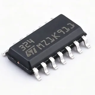
LM324ADR2G - Quad Op Amp, 3-32V, 1MHz SOIC-14 | onsemi
MPN: LM324ADR2G ✓ Active| Qty | Unit Price | Extended |
|---|---|---|
| 1 | $0.48 | $0.48 |
| 10 | $0.39 | $3.90 |
| 100 | $0.27 | $27.00 |
| 500 | $0.22 | $110.00 |
| 1,000 | $0.18 | $180.00 |
LM324ADR2G Overview
A quad operational amplifier is an integrated circuit that packs four identical, frequency-compensated op amp stages onto a single silicon die, sharing one set of power pins. Within the amplifier hierarchy, it belongs to the general-purpose bipolar op amp family: operational amplifier -> linear amplifier IC -> analog signal conditioning IC. Quad op amps reduce board area, cut per-channel cost, and improve channel-to-channel thermal matching versus four single op amps.
Key features include single-supply operation down to 3V with input common-mode range that includes ground - the defining trait that made the LM324 the industry-standard quad op amp. The A-grade suffix guarantees a maximum input offset voltage of 3 mV, tighter than the base LM324. Internally frequency compensation eliminates external compensation components, and the low supply current of approximately 700 µA per amplifier (typical for the family) suits battery-powered designs.
Technically, the LM324ADR2G uses a mature bipolar process with PNP input stages that enable ground-sensing inputs. The output stage is a classic single-ended Class-AB emitter follower, which means it can sink only limited current near ground and exhibits output crossover behavior under light loads - a known characteristic designers must account for in precision or audio paths.
Typical applications include transducer signal conditioning, DC gain blocks, active filters, comparators, voltage followers, and industrial sensor interfaces where single-supply, ground-referenced inputs simplify the power architecture.
Design consideration: keep total supply voltage within 32V, and remember the output cannot swing rail-to-rail - headroom of roughly 1.5V to the positive rail is required at moderate loads.
This page adds value beyond the manufacturer datasheet by synthesizing distributor pricing, verified drop-in alternatives, a parametric comparison table, and practical design notes in one place.
Drop-in alternatives for LM324ADR2G — same package, pin-to-pin compatible. Different-package parts requiring PCB rework are excluded.
Variants in this series
Same-series models that are drop-in compatible with LM324ADR2G (same form factor and footprint) — differing in Slew Rate, Input Offset Voltage, Package, Amplifier Type, Gain Bandwidth Product.
Quick Comparison Tool — Select alternative parts for side-by-side comparison:
LM324ADG
✅ Drop-In📋 Reference alternative (not in catalog)
LM324DT
✅ Drop-In✓ In Stock
$0.0827 / Unit
View Datasheet →LM324ADR
✅ Drop-In📋 Reference alternative (not in catalog)
LM324AIDR
✅ Drop-In📋 Reference alternative (not in catalog)
LM324ADT
✅ Drop-In📋 Reference alternative (not in catalog)
LM2904DR
✅ Drop-In✓ In Stock
$0.1 / Unit
View Datasheet →LM324ADR2G Maximum Ratings & Electrical Characteristics
| Amplifier Type | General Purpose |
| Number of Circuits | 4 |
| Supply Voltage Range (Single) | 3 V to 32 V |
| Supply Voltage Range (Split) | ±1.5 V to ±16 V |
| Gain Bandwidth Product | 1 MHz |
| Slew Rate | 0.6 V/µs |
| Input Offset Voltage (Max) | 3 mV |
| Technology | Bipolar |
| Package / Case | 14-SOIC (0.154in, 3.90mm Width) |
| Mounting Type | Surface Mount |
| Operating Temperature | 0C to +70C (Commercial) |
| Packaging | Tape & Reel (R2G suffix) |
LM324ADR2G Pin Configuration
| Pin 1 | OUT1 — Output of amplifier 1 |
| Pin 2 | IN1- — Inverting input, amplifier 1 |
| Pin 3 | IN1+ — Non-inverting input, amplifier 1 |
| Pin 4 | VCC — Positive supply pin |
| Pin 5 | IN2+ — Non-inverting input, amplifier 2 |
| Pin 6 | IN2- — Inverting input, amplifier 2 |
| Pin 7 | OUT2 — Output of amplifier 2 |
| Pin 8 | OUT3 — Output of amplifier 3 |
| Pin 9 | IN3- — Inverting input, amplifier 3 |
| Pin 10 | IN3+ — Non-inverting input, amplifier 3 |
| Pin 11 | GND/VEE — Ground (single supply) or negative rail (split supply) |
| Pin 12 | IN4+ — Non-inverting input, amplifier 4 |
| Pin 13 | IN4- — Inverting input, amplifier 4 |
| Pin 14 | OUT4 — Output of amplifier 4 |
Typical Applications
LM324ADR2G is suitable for 6 applications: Transducer Signal Conditioning, DC Gain Blocks and Level Shifting, Active Filters, Comparator and Window Detector Functions, Battery-Powered and Portable Instrumentation, Motor Drive and Power-Supply Supervision.
Transducer Signal Conditioning
Sensor bridges, thermistors, and current-sense shunts frequently produce ground-referenced signals in the millivolt range, and the LM324ADR2G is engineered precisely for this environment. Its input common-mode range extends to ground on a single 3V-32V supply, so a low-side shunt signal can be amplified without any negative rail or level-shifting circuitry. With the A-grade 3 mV maximum input offset voltage, gain stages up to about 100x keep offset-referred errors under 0.3V of output swing - acceptable for industrial monitoring thresholds. Designers should note the ~1.5V headroom to the positive rail when sizing output ranges, and the 1 MHz GBW limits closed-loop bandwidth to roughly 10 kHz at a gain of 100, which is ample for temperature, pressure, and light sensors that change slowly.
Recommended
DC Gain Blocks and Level Shifting
As a quad, the LM324ADR2G lets one package implement multi-stage gain chains - for example a difference amplifier followed by two gain stages and an active output buffer - cutting board area and BOM cost versus four single op amps. The internally compensated bipolar design is unconditionally stable at any gain setting, so no external compensation network is needed, simplifying layout. At unity gain the 1 MHz GBW delivers fast settling for slow control loops; at higher gains, bandwidth scales down linearly (100 kHz at gain of 10). Because the output stage is not rail-to-rail, reserve headroom of roughly 1.5V below VCC at moderate currents and expect the output to reach near 0V only under light sink currents - keep load impedances above about 10 kΩ when signals must approach ground.
Recommended
Active Filters
Multiple feedback low-pass, high-pass, and Sallen-Key filter sections fit naturally across the four channels of the LM324ADR2G, making it a compact analog front-end for anti-aliasing and noise conditioning ahead of ADCs. The 1 MHz gain-bandwidth product means filter corner frequencies up to a few tens of kilohertz are realized accurately at moderate Q; above roughly 100 kHz of unity-gain crossover, Q enhancement and phase errors appear as the amplifier's own pole intrudes, so limit designs to the audio and instrumentation band. The bipolar input bias current (nominally tens of nanoamperes) requires resistors in the 10 kΩ-100 kΩ range to keep offset errors small - use the A-grade 3 mV offset part and avoid megohm impedances that would convert bias current into significant DC error.
Recommended
Comparator and Window Detector Functions
The LM324ADR2G is commonly pressed into service as a low-cost comparator: open-collector-style behavior is not present, but with pull-down resistors or diode-OR outputs, quad channels implement window detectors, over-voltage monitors, and threshold comparators sharing one package. Ground-sensing inputs allow thresholds referenced to 0V on a single 5V-24V rail, a major simplification in industrial alarm circuits. Key cautions: the LM324 is not a specified comparator, so response time is in the low-microsecond range and phase reversal should be verified if inputs are driven beyond the common-mode range; add hysteresis of a few millivolts with positive feedback to prevent output chatter near the threshold caused by the 0.6 V/µs slew-limited transition.
Recommended
Battery-Powered and Portable Instrumentation
With operation down to 3V total supply and modest per-amplifier supply current typical of the family, the LM324ADR2G supports 3.3V-logic and single-cell lithium systems for portable meters and data loggers. The quad density multiplies channel count per package, and because all four amplifiers share one die, channel-to-channel offset and temperature tracking are inherently better than four separate packages - useful for differential measurements in handheld instruments. The trade-offs for battery designs are the non-rail-to-rail output (roughly 1.5V headroom) and bipolar bias currents higher than CMOS alternatives; keep source impedances moderate and design ADC ranges within the achievable output swing to avoid clipping near the top rail during low-battery conditions.
Recommended
Motor Drive and Power-Supply Supervision
In motor control and off-line power supplies, the LM324ADR2G is widely used for current-limit amplifiers, error amplifiers around feedback dividers, and fault supervision across its four channels - one package can monitor bus voltage, load current, and temperature while providing the control-loop error amplifier. Its 32V total supply ceiling allows direct connection to 24V industrial rails without pre-regulation, and ground-referenced inputs simplify low-side current-sense conditioning. The 0.6 V/µs slew rate and microsecond-class response suit slow protection loops, not fast cycle-by-cycle current limiting, so pair it with a dedicated fast comparator where sub-microsecond fault response is required. Supply the amplifier from a clean rail or add RC filtering, since PSRR in bipolar designs degrades at higher frequencies.
Recommended
Recommended Products Summary
Engineering reference data for LM324ADR2G — comparison, design guidance, and compliance information.
Selection Guide
Comparison with Alternatives
| Parameter | This Product | LM324ADG | LM324ADR | LM324AIDR | LM324ADT | LM2904DR |
|---|---|---|---|---|---|---|
| Package | SOIC-14 (3.90mm width) | SOIC-14 - same | SOIC-14 - same | SOIC-14 - same | SOIC-14 - same | SOIC-14 - same |
| Brand | onsemi | onsemi | Texas Instruments | Texas Instruments | STMicroelectronics | Texas Instruments |
| Number of Circuits | 4 | 4 | 4 | 4 | 4 | 4 |
| Supply Voltage Range (Single) | 3 V to 32 V | 3 V to 32 V | 3 V to 32 V | 3 V to 32 V | 3 V to 32 V | 3 V to 32 V |
| Gain Bandwidth Product | 1 MHz | 1 MHz | 1 MHz | 1 MHz | 1 MHz | 1 MHz |
| Slew Rate | 0.6 V/µs | 0.6 V/µs | 0.5 V/µs | 0.5 V/µs | 0.5 V/µs | 0.5 V/µs |
| Operating Temperature | 0C to +70C | 0C to +70C | 0C to +70C | -40C to +85C | 0C to +70C | -40C to +125C |
Key Differentiators
- A-grade offset accuracy at commodity price (vs LM324D (onsemi base grade))
- Ground-sensing inputs on a single supply (vs TL074 (JFET-input SOIC-14 quad))
- Drop-in cross-brand supply resilience (vs LM324ADR / LM324AIDR (Texas Instruments))
Design Notes
The LM324 output stage is not rail-to-rail: at moderate loads the output saturates roughly 1.5V below VCC, and near ground it can only sink a small current. Do not design signal ranges that assume the output reaches the positive rail, and keep feedback networks light (10 kΩ or higher) so the output can pull close to ground. Driving the output toward ground into a load referenced to a negative or mid rail can also cause the output stage to draw excessive current. These are classic LM324 family behaviors documented across manufacturer application notes.
Place a 100 nF ceramic decoupling capacitor directly across pins 4 (VCC) and 11 (GND/VEE), within a few millimeters of the package, plus bulk capacitance per board practice. Keep high-impedance input traces (pins 2, 3, 5, 6, 9, 10, 12, 13) short and guard them away from output traces to prevent unintended feedback paths, especially with the four channels sharing one die where crosstalk can occur between adjacent amplifiers (for example OUT2 on pin 7 next to OUT3 on pin 8). Ground-referenced input layouts benefit from a clean analog ground region under the IC.
Estimated: the total supply voltage must never exceed 32V across pins 4 and 11. On a 24V industrial rail, this leaves only 8V margin - verify worst-case transients and add a series resistor plus zener clamp or a small pre-regulator if surges are possible. Estimated supply current is on the order of 1-3 mA for all four amplifiers at mid-supply, so self-heating in the SOIC-14 is negligible; thermal design is not required, but supply sequencing with respect to input signals should avoid inputs exceeding the positive rail during startup.
Compliance Information
The onsemi 'G' suffix in LM324ADR2G conventionally denotes lead-free/RoHS-compliant termination per onsemi part numbering, but explicit RoHS/REACH certification status was not stated in the provided verified web data and is therefore marked unknown.