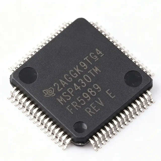
MSP430FR5989IPMR - 128KB FRAM 16MHz Rotary Sensing MCU | TI
MPN: MSP430FR5989IPMR ✓ Active| Qty | Unit Price | Extended |
|---|---|---|
| 1 | $8.6 | $8.60 |
| 10 | $8.2 | $82.00 |
| 100 | $7.4 | $740.00 |
| 500 | $6.8 | $3,400.00 |
| 1,000 | $6.3 | $6,300.00 |
MSP430FR5989IPMR Overview
A microcontroller (MCU) is a compact integrated circuit that combines a processor core, program memory, data memory, and programmable peripherals on a single die to govern a specific embedded function. Within the MCU hierarchy, this device belongs to the MSP430 FRAM family of ultra-low-power (ULP) microcontrollers under the broader MSP430 platform and power-management IC taxonomy. Its FRAM (ferroelectric RAM) memory unites SRAM-like speed, flexibility, and endurance with flash-like non-volatility at much lower write energy, eliminating the erase-before-write cycles of conventional flash.
Key features include the extended Scan Interface 2 that offloads high-resolution rotary and linear position sensing from the CPU, a hardware AES accelerator for secure metering data, a real-time clock with calendar mode, a 12-bit ADC, comparator, DMA controller, a 32-bit hardware multiplier, and multiple 16-bit timers. Power performance is exceptional: active mode draws approximately 100 uA/MHz and standby (LPM3 with VLO) about 0.4 uA, enabling decade-class battery life in field instruments.
Architecturally, the CPUXV2 core executes a 16-bit RISC instruction set over a von Neumann bus at 16MHz. FRAM is byte-writable in-system, allowing fast data logging without external EEPROM, while the AES accelerator encrypts measurements for smart-grid and flow-metering security. The operating supply range is 1.8V to 3.6V with -40C to +85C temperature tolerance for harsh deployments.
Typical applications include gas, water, and heat flow meters, rotary and linear position sensing systems, smart-grid endpoints, industrial process control, and secure wireless sensor nodes. Scan Interface 2 directly supports rotary encoders while the CPU sleeps, minimizing average current.
Design tip: decouple each VCC pin with 100nF close to the pin plus 10uF bulk capacitance, keep the supply above the SVS threshold for reliable FRAM writes, and use JTAG or two-wire Spy-Bi-Wire for debugging.
This page synthesizes distributor pricing, drop-in alternatives, and practical design notes not found in the manufacturer datasheet.
Drop-in alternatives for MSP430FR5989IPMR — same package, pin-to-pin compatible. Different-package parts requiring PCB rework are excluded.
Variants in this series
Same-series models that are drop-in compatible with MSP430FR5989IPMR (same form factor and footprint) — differing in Package, ADC Resolution, Data Bus Width, SRAM, Timers.
Quick Comparison Tool — Select alternative parts for side-by-side comparison:
MSP430FR5994IPMR
✅ Drop-In ⚠️ Specs Unverified✓ In Stock
$4.21 / Unit
View Datasheet →MSP430FR5988IPMR
✅ Drop-In ⚠️ Specs Unverified📋 Reference alternative (not in catalog)
MSP430FR5987IPMR
✅ Drop-In ⚠️ Specs Unverified📋 Reference alternative (not in catalog)
MSP430FR6989IPMR
✅ Drop-In ⚠️ Specs Unverified📋 Reference alternative (not in catalog)
MSP430FR6879IPMR
✅ Drop-In ⚠️ Specs Unverified📋 Reference alternative (not in catalog)
MSP430FR5989IPMR Maximum Ratings & Electrical Characteristics
| Core Processor | MSP430 CPUXV2 16-bit RISC |
| Core Size | 16-bit |
| Maximum Clock Frequency | 16 MHz |
| Program Memory Type | FRAM |
| Program Memory Size | 128 KB (128K x 8) |
| RAM Size | 2 KB |
| Supply Voltage Range | 1.8 V to 3.6 V |
| Active Mode Current | approx. 100 uA/MHz |
| Standby Current (LPM3 with VLO) | approx. 0.4 uA |
| Peripherals | Extended Scan Interface 2, AES accelerator, RTC, DMA, 32-bit hardware multiplier, comparator |
| ADC Resolution | 12-bit |
| Operating Temperature | -40C to +85C |
| Package | 64-LQFP (PM) 10x10 mm |
| Mounting Type | Surface Mount |
| Debug Interface | JTAG, Spy-Bi-Wire (2-wire) |
| Packaging | Tape & Reel (R suffix) |
MSP430FR5989IPMR 64-lqfp (pm) 10x10 mm Pin Configuration Guide
Pin configuration for MSP430FR5989IPMR (64-lqfp (pm) 10x10 mm package). This digital IC includes GPIO, communication interfaces (UART, SPI, I2C), and power pins. Refer to the manufacturer datasheet for alternate pin functions and configuration options. Essential for embedded system design and PCB layout.

No detailed pinout data available for MSP430FR5989IPMR.
Refer to the datasheet for full pin configuration.
Typical Applications
MSP430FR5989IPMR is suitable for 6 applications: Smart Gas and Water Flow Meters, Rotary and Linear Position Sensing, Smart Grid Endpoint Devices, Industrial Process Control Nodes, Secure Wireless Sensor Nodes, Heat and Thermal Energy Metering.
Smart Gas and Water Flow Meters
The MSP430FR5989IPMR fits battery-powered flow metering because its extended Scan Interface 2 monitors rotary encoder transitions autonomously while the CPU sleeps at roughly 0.4 uA in LPM3, and active code runs at about 100 uA/MHz. FRAM's low write energy allows frequent logging of consumption profiles without the erase-cycle overhead and higher write current of flash. The hardware AES accelerator encrypts usage data for secure smart-grid billing, and 1.8V operation lets the design extract full life from primary lithium cells. Typical topology: ESI2 samples the encoder, wakes the CPU on rotation events, logs volume to FRAM, and transmits via an external RF or M-Bus link. The -40C to +85C range covers unsheltered outdoor installations.
Recommended
Rotary and Linear Position Sensing
For rotary encoders, valve position feedback, and linear displacement sensing, the MSP430FR5989IPMR's Scan Interface 2 performs autonomous multi-channel sensor scanning with hardware threshold decisions, offloading this periodic task from the CPU. This means the 16MHz CPUXV2 core only wakes when a qualified position change occurs, cutting average system current by orders of magnitude versus software polling. The 12-bit ADC supports analog sensor fronts, while the 32-bit hardware multiplier accelerates position-to-angle conversion math. Calibration constants and lookup tables live in byte-writable FRAM, so field calibration updates need no external EEPROM. In industrial automation nodes, pairing the MCU with an isolated transceiver such as the AM2632-Q1 provides a robust fieldbus interface.
Recommended
Smart Grid Endpoint Devices
Smart-grid endpoints - electricity meter auxiliary boards, concentrators, and district-heat interfaces - benefit from the MSP430FR5989IPMR's combination of security and ultra-low power. The AES hardware accelerator encrypts measured consumption and authentication messages without software crypto overhead, while the RTC with calendar mode maintains tariff schedules at standby currents near 0.4 uA. FRAM endurance supports decades of interval-data logging at 15-minute measurement periods without memory wear concerns. The 1.8V to 3.6V supply range tolerates battery backup sag during mains outages. Designers typically pair it with TI C2000 metrology DSPs such as the TMS320F280041C-Q1 in the main metering stage, using the FR5989 as the low-power communication and tamper-detection controller.
Recommended
Industrial Process Control Nodes
In distributed industrial process control, the MSP430FR5989IPMR serves as a low-power sensor node controller reading 4-20 mA loops, thermistors, or pulse-output flow sensors through its 12-bit ADC and timers. Its 16MHz core handles PID trim calculations, while DMA moves conversion results without CPU cycles. FRAM retains setpoints and diagnostics through power interruptions without battery-backed SRAM. Standby near 0.4 uA suits loop-powered and energy-harvesting installations where every microamp counts. The -40C to +85C rating tolerates control-cabinet environments. For higher compute demands, the node can pair with a C2000 real-time controller such as the TMS320F28335PTPQ handling the main control loop while the FR5989 manages communication, logging, and housekeeping duties.
Recommended
Secure Wireless Sensor Nodes
Battery-powered wireless sensor nodes use the MSP430FR5989IPMR as the main controller because its active current around 100 uA/MHz and LPM3 standby of about 0.4 uA maximize battery life between radio bursts. The AES accelerator encrypts payloads for over-the-air privacy, and FRAM's byte-writability supports frequent sensor-state checkpointing so the node can resume exactly after sleep or reset. The 12-bit ADC and comparator handle direct sensor attachment, and the 32-bit hardware multiplier accelerates filtering math before transmission. Combined with a sub-1GHz or 2.4GHz RF transceiver, the node wakes on a timer or sensor interrupt, samples, encrypts, and transmits within milliseconds. The 64-pin LQFP provides enough GPIO for multiple sensors plus the radio interface on one footprint.
Recommended
Heat and Thermal Energy Metering
District heat and thermal energy meters pair a flow sensor with paired temperature probes; the MSP430FR5989IPMR suits this role because its 12-bit ADC digitizes PT500/PT1000 bridge signals, its RTC maintains metering intervals at micropower standby, and FRAM logs accumulated energy with minimal write energy. The Scan Interface 2 reads the rotary or ultrasonic flow element autonomously, keeping average current low enough for a 10+ year lithium battery service target. The AES accelerator secures billing data per utility requirements, and operation down to 1.8V accommodates aging cells. The extended temperature range covers plant rooms and buried chambers. TI reference metering designs demonstrate this architecture with the FR59xx family as the computing core.
Recommended
Recommended Products Summary
Engineering reference data for MSP430FR5989IPMR — comparison, design guidance, and compliance information.
Selection Guide
Comparison with Alternatives
| Parameter | This Product | MSP430FR5994IPMR | MSP430FR5988IPMR | MSP430FR5987IPMR | MSP430FR6989IPMR |
|---|---|---|---|---|---|
| Package | 64-LQFP (PM) 10x10 mm | 64-LQFP (PM) - same | 64-LQFP (PM) - same | 64-LQFP (PM) - same | 64-LQFP (PM) - same |
| Brand | Texas Instruments | Texas Instruments | Texas Instruments | Texas Instruments | Texas Instruments |
| Program Memory (FRAM) | 128 KB | 256 KB | 96 KB | 64 KB | 128 KB |
| Core / Max Clock | MSP430 CPUXV2 / 16 MHz | MSP430 CPUXV2 / 16 MHz | MSP430 CPUXV2 / 16 MHz | MSP430 CPUXV2 / 16 MHz | MSP430 CPUXV2 / 16 MHz |
| Supply Voltage | 1.8 V to 3.6 V | 1.8 V to 3.6 V | 1.8 V to 3.6 V | 1.8 V to 3.6 V | 1.8 V to 3.6 V |
| Operating Temperature | -40C to +85C | -40C to +85C | -40C to +85C | -40C to +85C | -40C to +85C |
Key Differentiators
- Extended Scan Interface 2 for autonomous rotary sensing (vs MSP430FR6989IPMR)
- 256KB FRAM upgrade path on same footprint (vs MSP430FR5994IPMR)
- Balanced memory/cost point in FR59xx family (vs MSP430FR5987IPMR)
Design Notes
Decouple every VCC pin with a 100nF ceramic capacitor placed within 2mm of the pin, plus at least 10uF of bulk capacitance near the 64-LQFP supply entry. Keep the supply above the SVS (supply voltage supervisor) threshold during FRAM writes; a brownout mid-write can corrupt the affected FRAM word. Estimated: at 3.3V and 16MHz active, current is roughly 1.6 mA (100 uA/MHz), so a 2400mAh lithium cell theoretically supports years of intermittent operation if LPM3 duty cycle dominates.
Route the Spy-Bi-Wire (SBWTCK/SBWTDIO) test pads to a standard 2x5-pin cTI header even in production boards; in-field firmware updates without this access require full disassembly. Keep the analog reference and ADC input traces away from the ESI2 sensor lines, and use a solid ground plane under the 10x10mm QFP. The thermal pad considerations are minimal for this low-power MCU, but pour ground under the package to reduce ground bounce on the 12-bit ADC.
Do not assume flash-style code: FRAM is byte-writable without erase, but writes require the FRCTL wait-state configuration for CPU speeds above 8MHz per TI family guidance - misconfiguration causes hard faults. Also, LPM3 current figures quoted (approx. 0.4 uA) assume VLO clock and all unused GPIO configured as outputs or with pull resistors; floating inputs can each leak microamps, silently destroying battery-life budgets in metering designs.
Extended Scan Interface 2 sensor lines are sensitive comparator inputs; route encoder signals as short twisted pairs or guarded traces, and add RC filtering matched to the expected rotation frequency. Estimated: for a 10kHz maximum encoder pulse rate, a 1k ohm / 1nF RC gives roughly a 160kHz corner, preserving pulse edges while rejecting broadband noise from nearby switching converters.
Compliance Information
RoHS compliance and lead-free finish per standard TI catalog MCU product data; detailed REACH/halogen status should be confirmed on the TI product page quality portal.







