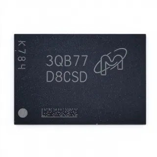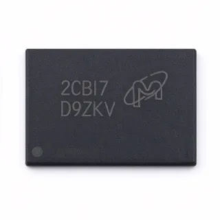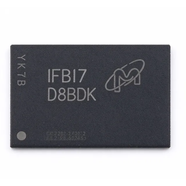
MT53E256M16D1FW-046 - 4Gb LPDDR4X SDRAM 2133MHz | Micron
MPN: MT53E256M16D1FW-046 ✓ Active| Qty | Unit Price | Extended |
|---|---|---|
| 1 | $9.33 | $9.33 |
| 10 | $8.87 | $88.70 |
| 100 | $8.21 | $821.00 |
| 500 | $7.65 | $3,825.00 |
| 1,000 | $7.2 | $7,200.00 |
MT53E256M16D1FW-046 Overview
LPDDR4X (Low Power Double Data Rate 4X) is a JEDEC-defined mobile DRAM standard that evolved from LPDDR4 to reduce the I/O interface voltage from 1.1V down to 0.6V VDDQ, dramatically lowering I/O power consumption. In the memory hierarchy, LPDDR4X sits in the family of low-power synchronous DRAMs (LPDRAM) alongside LPDDR4, LPDDR5, and wide-I/O, serving as the main system memory where power efficiency is critical. Unlike desktop DDR, LPDDR devices are soldered directly onto the PCB, so package, ballout, and controller compatibility must be fixed at board design time.
Key features of this device include 4Gbit density in a single die, x16 data width for simplified bus routing, a 2133 Mbps/pin data rate, and LPDDR4X low-voltage I/O operation at 0.6V VDDQ with a 1.1V core supply. Extended temperature variants (-AAT, -AIT, -AUT suffixes) support industrial and automotive deployment.
Architecturally, the MT53E256M16D1FW-046 uses Micron LPDDR4X DRAM core technology with bank groups enabling high-speed burst transfers at low latency. On-die termination, DQ Vref training, and low-power self-refresh modes (with deep power-down) minimize standby draw, which is essential for battery-powered designs. Per-ball impedance control and controlled slew rates support signal integrity at 2133 Mbps.
Typical applications include mobile phone and tablet main memory, embedded and IoT gateways, automotive infotainment and ADAS domains, networking equipment buffers, and portable medical devices where low power per bit is a primary selection criterion.
Design consideration: because LPDDR4X trace length and impedance matching dominate signal integrity, follow Micron's reference PCB layout guidelines - length-match data lanes within the datasheet skew budget and place the device within the controller's fly-by window.
This page synthesizes distributor pricing, same-package temperature-grade alternatives, and practical design guidance not consolidated in the manufacturer datasheet.
Drop-in alternatives for MT53E256M16D1FW-046 — same package, pin-to-pin compatible. Different-package parts requiring PCB rework are excluded.
Variants in this series
Same-series models that are drop-in compatible with MT53E256M16D1FW-046 (same form factor and footprint) — differing in Data Rate, Density, Interface, Memory Type, Mounting Type.
Quick Comparison Tool — Select alternative parts for side-by-side comparison:
MT53E256M16D1FW-046 AAT:B
📋 Reference alternative (not in catalog)
MT53E256M16D1FW-046 AIT:B
📋 Reference alternative (not in catalog)
MT53E256M16D1FW-046 AUT:B
📋 Reference alternative (not in catalog)
MT53E256M16D1FW-046 WT ES:B
📋 Reference alternative (not in catalog)
MT53E256M16D1FW-046 Maximum Ratings & Electrical Characteristics
| Memory Type | SDRAM - Mobile LPDDR4X |
| Density | 4 Gbit |
| Organization | 256M x 16 |
| Data Rate | 2133 Mbps/pin (2.133 GHz) |
| Clock Cycle Time | 3.5 ns |
| Core Supply Voltage (VDD) | 1.1 V |
| I/O Supply Voltage (VDDQ) | 0.6 V (LPDDR4X) |
| Interface | Parallel |
| Package | 200-TFBGA (10 x 14.5 mm) |
| Mounting Type | Surface Mount (BGA soldered) |
| Technology | LPDDR4X LPDRAM |
| Speed Grade | -046 (2133 MHz class) |
| Ball Count | 200 |
| Package Dimensions | 10 mm x 14.5 mm |
| Low Power Modes | Self-refresh, deep power-down, DPD |
MT53E256M16D1FW-046 10 mm x 14.5 mm Pin Configuration Guide
Pin configuration for MT53E256M16D1FW-046 (10 mm x 14.5 mm package). This digital IC includes GPIO, communication interfaces (UART, SPI, I2C), and power pins. Refer to the manufacturer datasheet for alternate pin functions and configuration options. Essential for embedded system design and PCB layout.

No detailed pinout data available for MT53E256M16D1FW-046.
Refer to the datasheet for full pin configuration.
Typical Applications
MT53E256M16D1FW-046 is suitable for 6 applications: Smartphone and Tablet Main Memory, Automotive Infotainment and ADAS, Industrial IoT Gateways and Edge Computing, Networking Equipment Buffer Memory, Portable Medical and Wearable Devices, Embedded Vision and Camera Systems.
Smartphone and Tablet Main Memory
The MT53E256M16D1FW-046 is purpose-built for mobile main memory: its 4Gbit (512 MB) density covers mid-tier smartphone OS footprints, the x16 organization simplifies SoC bus routing to a single 16-bit channel, and LPDDR4X 0.6V VDDQ halves I/O switching power versus LPDDR4 at the same 2133 Mbps/pin rate. Mounted in the 200-TFBGA (10 x 14.5 mm) footprint directly beneath or beside the application processor, it typically operates at 1.1V VDD / 0.6V VDDQ from a PMIC LPDDR rail. Performance depends on trace-length matching within the datasheet skew budget; deep power-down and self-refresh modes minimize standby drain when the screen is off, directly extending battery life.
Recommended
Automotive Infotainment and ADAS
In automotive IVI head units and ADAS domain controllers, the AUT:B temperature-grade variant of this same die provides Micron automotive qualification with identical 4Gbit/2133 Mbps performance in the identical 200-ball TFBGA footprint, so the PCB can be shared across consumer and automotive builds. The MT53E256M16D1FW-046 class of LPDDR4X supplies the frame buffers and working set for camera pipelines, navigation rendering, and voice processing, where 0.6V VDDQ reduces rail power in fanless enclosures. Design consideration: automotive power trees must sequence VDD (1.1V) before VDDQ (0.6V) per datasheet requirements, and extended-temperature derating of the -046 speed grade should be verified against the AEC-qualified timing tables.
Recommended
Industrial IoT Gateways and Edge Computing
Industrial gateways running Linux-class SoCs need 512 MB-class memory with industrial qualification; the AIT:B and AAT:B grades of this exact die deliver that with the same 200-TFBGA (10 x 14.5 mm) footprint and 2133 Mbps/pin bandwidth for packet buffering, TLS sessions, and local analytics. The MT53E256M16D1FW-046 LPDDR4X organization (256M x16) pairs cleanly with single-channel ARM Cortex-A SoCs. Thermal design matters in sealed enclosures: the BGA dissipates modest power (1.1V core, 0.6V I/O), but junction temperature must stay within the industrial grade limit at high ambient. Self-refresh mode retains memory contents during gateway low-power wake windows with microwatt-class standby draw.
Recommended
Networking Equipment Buffer Memory
Switch, router, and CPE designs use LPDDR4X as packet-buffer and control-plane memory. The MT53E256M16D1FW-046 provides 2133 Mbps/pin bandwidth (about 4.2 GB/s peak on a x16 channel), which sustains line-rate buffering for gigabit-class traffic with headroom for management CPU workloads. Its x16 organization allows single-component designs on compact CPE boards, while 0.6V VDDQ helps meet whole-system power budgets in passively cooled outdoor customer-premises equipment. Layout guidance: keep the 200-ball TFBGA within the controller's specified trace-length window and maintain datasheet-referenced DQ strobe matching, as buffer bandwidth at 2133 Mbps is sensitive to lane skew.
Recommended
Portable Medical and Wearable Devices
Battery-powered patient monitors, portable diagnostics, and high-end wearables benefit from the MT53E256M16D1FW-046's low I/O voltage: at 0.6V VDDQ the LPDDR4X interface cuts I/O power approximately in half compared to LPDDR4 at 1.1V, reducing heat near the skin contact surface and extending run time. The 512 MB capacity comfortably hosts an embedded OS plus signal-processing working sets for ECG/SpO2 pipelines, while deep power-down mode drops standby consumption to the low-microamp range between measurements. The compact 200-TFBGA (10 x 14.5 mm) footprint fits small main boards; all temperature-grade variants share the same ballout, simplifying medical-to-consumer platform reuse.
Recommended
Embedded Vision and Camera Systems
Embedded vision modules (smart cameras, robot vision, video doorbells) stream sensor frames through ISP and AI accelerators that demand sustained memory bandwidth; the MT53E256M16D1FW-046's 2133 Mbps/pin x16 channel delivers roughly 4.2 GB/s peak, adequate for 1080p30 pipelines with a compact CNN inference working set. LPDDR4X 0.6V VDDQ reduces switching noise on the analog front end, and the 1.1V/0.6V rails integrate with standard PMIC LPDDR outputs. Signal integrity is the dominant design factor: the 200-ball TFBGA layout must follow length-matched fly-by routing and datasheet termination guidelines. Self-refresh enables instant-on capture with minimal wake latency between frames.
Recommended
Recommended Products Summary
Engineering reference data for MT53E256M16D1FW-046 — comparison, design guidance, and compliance information.
Selection Guide
Comparison with Alternatives
| Parameter | This Product | MT53E256M16D1FW-046 AAT | MT53E256M16D1FW-046 AIT | MT53E256M16D1FW-046 AUT | MT53E256M16D1FW-046 WT ES |
|---|---|---|---|---|---|
| Package | 200-TFBGA (10 x 14.5 mm) | B: 200-TFBGA (10 x 14.5 mm) - same | B: 200-TFBGA (10 x 14.5 mm) - same | B: 200-TFBGA (10 x 14.5 mm) - same | B: 200-TFBGA (10 x 14.5 mm) - same |
| Brand | Micron Technology | B: Micron Technology | B: Micron Technology | B: Micron Technology | B: Micron Technology |
| Density | 4 Gbit | B: 4 Gbit | B: 4 Gbit | B: 4 Gbit | B: 4 Gbit |
| Organization | 256M x 16 | B: 256M x 16 | B: 256M x 16 | B: 256M x 16 | B: 256M x 16 |
| Data Rate | 2133 Mbps/pin | B: 2133 Mbps/pin | B: 2133 Mbps/pin | B: 2133 Mbps/pin | B: 2133 Mbps/pin |
| Temperature Grade | WT (standard mobile) | B: AT (industrial extended) | B: IT (industrial) | B: AUT (automotive) | B: WT engineering sample |
| VDDQ I/O Voltage | 0.6 V (LPDDR4X) | B: 0.6 V (LPDDR4X) | B: 0.6 V (LPDDR4X) | B: 0.6 V (LPDDR4X) | B: 0.6 V (LPDDR4X) |
| Production Status | Production | B: Production | B: Production | B: Production | B: Engineering sample - not for production |
Key Differentiators
- LPDDR4X 0.6V VDDQ halves I/O power (vs MT53D-series LPDDR4 predecessors)
- One footprint across all qualification grades (vs MT53E256M16D1FW-046 AUT:B)
- Trade-off: single-vendor drop-in only (vs Cross-brand 4Gb x16 LPDDR4X)
Design Notes
At 2133 Mbps/pin, LPDDR4X signal integrity is dominated by trace-length matching and reference-plane continuity. Length-match all DQ/DQS lanes within the datasheet skew budget, keep the 200-TFBGA within the controller's specified routing window, and follow Micron's LPDDR4/4X system design guidelines for fly-by address/command routing. Use ODT and Vref training during boot as provided by the SoC memory controller. Estimated: every 10 mm of unmatched trace can introduce tens of picoseconds of skew at these data rates, eroding timing margin.
Power the device with 1.1V VDD (core) and 0.6V VDDQ (LPDDR4X I/O) rails from a PMIC with proper power-up sequencing per the datasheet - VDD must be stable before or with VDDQ. Add bulk capacitance plus local high-frequency decoupling at each rail near the BGA; the 0.6V VDDQ rail carries the bulk of switching current at 2133 Mbps, so low-ESR ceramics placed within a few millimeters of the ball fanout are essential. Avoid sharing VDDQ with other noise-sensitive loads.
Do not assume cross-vendor LPDDR4X pin compatibility: ballouts are vendor-set, and swapping to a competing 4Gb x16 part generally requires a PCB re-spin plus controller firmware re-training. Also distinguish ordering suffixes - WT, AAT, AIT, AUT, and WT ES (engineering sample) - and never release ES silicon to production. Confirm the SoC vendor's memory compatibility list includes the MT53E256M16D1FW-046 exact speed grade before layout freeze.
Compliance Information
Compliance status not stated in the provided web data. The AUT:B variant follows Micron's automotive qualification flow, but specific AEC-Q100 status for this MPN is not stated in the provided data - consult the Micron product page.