MT53E1G32D2FW-046 - 32Gbit LPDDR4X SDRAM 200-TFBGA | Micron
MPN: MT53E1G32D2FW-046 ✓ Active| Qty | Unit Price | Extended |
|---|---|---|
| 1 | $295.93 | $295.93 |
| 10 | $305 | $3,050.00 |
| 100 | $315 | $31,500.00 |
| 500 | $330 | $165,000.00 |
| 1,000 | $341.88 | $341,880.00 |
MT53E1G32D2FW-046 Overview
LPDDR4X (Low Power Double Data Rate 4X) is a JEDEC-standardized mobile DRAM technology that reduces the I/O voltage (VDDQ) to 0.6V compared with the 1.1V VDDQ of standard LPDDR4, cutting I/O power consumption by roughly 40 percent. In the memory hierarchy, it sits as a high-bandwidth main-memory component between the application processor and storage (NAND flash), providing the working memory for SoC-based systems.
Key features include 32Gbit density in a dual-die (DDP) configuration with two independent 16-bit channels, the -046 speed grade supporting 4266 Mb/s per pin, auto self-refresh with a built-in temperature sensor, auto precharge, write leveling, and ZQ calibration functions. The 0.6V VDDQ combined with deep power-down and self-refresh modes makes the device especially attractive for battery-powered designs where every milliwatt matters.
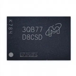
Architecturally, the part uses Micron 1x-nm class DRAM process technology with two dies stacked in the same 200-ball package. Die revisions :A (FBGA code D9ZQX) and :B (FBGA code D8CJB) circulate in the market; both share identical package dimensions, speed grade, and electrical interface but are covered by different datasheets, a detail engineers should verify atIncoming-inspection time.
Typical applications include automotive infotainment and ADAS platforms (the AUT temperature variants are specified from -40C to +125C), mobile smartphones and tablets, industrial HMI and edge-AI compute modules, and networking equipment.
Design consideration: because LPDDR4X VDDQ is 0.6V, this part is NOT a plug-and-play drop-in for standard LPDDR4 (1.1V VDDQ) predecessors such as MT53D1024M32D4DT; controller firmware, PMIC rails, and termination settings must be validated.
This page synthesizes distributor pricing, same-footprint alternatives, and practical design notes not found in the manufacturer datasheet. Pricing references are as of 2026-09-02.
Drop-in alternatives for MT53E1G32D2FW-046 — same package, pin-to-pin compatible. Different-package parts requiring PCB rework are excluded.
Variants in this series
Same-series models that are drop-in compatible with MT53E1G32D2FW-046 (same form factor and footprint) — differing in Memory Type, Organization, Clock Frequency, Memory Size, Package.
Quick Comparison Tool — Select alternative parts for side-by-side comparison:
MT53E1G32D2FW-046 WT:C
✅ Drop-In📋 Reference alternative (not in catalog)
MT53E1G32D2FW-046 AUT:B
✅ Drop-In✓ In Stock
$273.51 / Unit
View Datasheet →MT53E1G32D2FW-046 AAT:B
✅ Drop-In📋 Reference alternative (not in catalog)
MT53E1G32D2FW-046 AIT:B
✅ Drop-In📋 Reference alternative (not in catalog)
MT53E512M32D2FW-046 AAT:D
✅ Drop-In ⚠️ Specs Unverified✓ In Stock
$13.75 / Unit
View Datasheet →K4FBE3D4HM-TFCL
✅ Drop-In📋 Reference alternative (not in catalog)
MT53E1G32D2FW-046 Maximum Ratings & Electrical Characteristics
| Memory Type | Mobile LPDDR4X SDRAM |
| Memory Size | 32 Gbit (4 GB) |
| Organization | 1G x 32 (dual-die, 2 x 16-bit channels) |
| Interface | Parallel |
| Clock Frequency | 2133 MHz (2.133 GHz) |
| Data Rate | 4266 Mb/s per pin |
| Access Time | 3.5 ns |
| Write Cycle Time | 18 ns |
| VDDQ I/O Voltage | 0.6 V |
| Package | 200-TFBGA (10 x 14.5 mm) |
| Ball Diameter | 0.40 mm (SMD balls) |
| Mounting Type | Surface Mount |
| Operating Temperature (AUT variant) | -40C to +125C |
| Die Revisions | :A (FBGA D9ZQX) and :B (FBGA D8CJB) |
| Features | Auto self-refresh, built-in temperature sensor, auto precharge, write leveling, ZQ calibration |
MT53E1G32D2FW-046 200-tfbga (10 x 14.5 mm) Pin Configuration Guide
Pin configuration for MT53E1G32D2FW-046 (200-tfbga (10 x 14.5 mm) package). This digital IC includes GPIO, communication interfaces (UART, SPI, I2C), and power pins. Refer to the manufacturer datasheet for alternate pin functions and configuration options. Essential for embedded system design and PCB layout.

No detailed pinout data available for MT53E1G32D2FW-046.
Refer to the datasheet for full pin configuration.
Typical Applications
MT53E1G32D2FW-046 is suitable for 6 applications: Automotive ADAS and Infotainment, Mobile Smartphones and Tablets, Industrial Edge-AI Compute Modules, Networking and Enterprise Equipment, Consumer Electronics and Smart Displays, Test and Measurement Instruments.
Automotive ADAS and Infotainment
The MT53E1G32D2FW-046 AUT:B and AIT:B suffixes are specified from -40C to +125C with Micron's automotive manufacturing flow, making them suitable for camera-fusion ADAS domains and cockpit infotainment SoCs that need multi-GB working memory. The 32Gbit density across two 16-bit channels at 4266 Mb/s delivers roughly 17 GB/s of peak bandwidth per channel-pair, sufficient for sensor-fusion workloads. The built-in temperature sensor and auto self-refresh keep refresh overhead low across the automotive thermal envelope. Designers must connect the 0.6V VDDQ rail from an AEC-qualified PMIC and validate memory training at cold crank and hot-soak conditions, since LPDDR4X training tables shift over temperature.
Recommended
Mobile Smartphones and Tablets
The WT suffixes of the MT53E1G32D2FW-046 target mobile flagship designs where 4GB of LPDDR4X main memory and the 0.6V VDDQ I/O rail cut I/O power roughly 40 percent versus 1.1V LPDDR4 - directly extending battery life in standby-heavy usage. The 1G x 32 organization matches typical application-processor 32-bit memory controllers, and the dual-die package keeps PCB area to 10 x 14.5 mm. Because the package uses 0.40 mm SMD balls, standard fine-pitch BGA assembly is used. Designers should place the PMIC within a few tens of millimeters of the ballout to keep the VDD2/VDDQ distribution low-impedance and route DQ/CA length-matched per Micron's package layout guide.
Recommended
Industrial Edge-AI Compute Modules
The AIT (industrial) suffix of the MT53E1G32D2FW-046 serves edge-AI SOMs and industrial HMIs that need large frame buffers and model workspace memory. With 4GB of LPDDR4X at 4266 Mb/s, the part feeds NPUs and GPU-class accelerators that stream activation tensors continuously; the two-channel architecture lets one channel serve the display pipeline while the other serves inference workloads. The built-in temperature sensor enables temperature-compensated refresh across -40C to +85C industrial ambients, and auto precharge reduces controller overhead in random-access-heavy workloads. Designers typically pair the DRAM with an industrial SoC and verify Eye diagrams at the connector if the memory is on a module-to-carrier interface.
Recommended
Networking and Enterprise Equipment
Switches, routers, and 5G small-cell platforms use the MT53E1G32D2FW-046 as deep packet-buffer and control-plane memory alongside the network processor. The 32Gbit density reduces DRAM chip count on control cards, and 4266 Mb/s operation sustains queue-management bursts without becoming the bottleneck. The ZQ calibration function maintains output impedance accuracy across temperature, which matters in fan-cooled equipment with wide thermal swings. Because networking boards often run 24/7, designers should enable auto self-refresh during idle periods to cut DRAM background power, and they should verify the read ODT setting against the trace topology of their memory bus to keep signal integrity within the JEDEC LPDDR4X mask.
Recommended
Consumer Electronics and Smart Displays
Smart displays, TV set-top boxes, and streaming media players use the WT suffixes of the MT53E1G32D2FW-046 to provide 4GB of main memory for 4K video decode buffers and application runtimes. The dual-channel 32-bit aggregate bus at 4266 Mb/s comfortably sustains multi-stream 4K60 decode plus UI composition. LPDDR4X's deep power-down mode supports the fast-wake standby behavior consumers expect, dropping DRAM power to microamps while retaining the ability to resume in milliseconds. Cost-sensitive consumer designs should evaluate the WT:B versus WT:C suffix availability at their build site, since the two flow variants trade unit price against supply continuity. Verify die revision :A versus :B at incoming inspection when dual-sourcing reels.
Recommended
Test and Measurement Instruments
Oscilloscopes and logic analyzers require deep acquisition memory; the MT53E1G32D2FW-046 provides 4GB of LPDDR4X that instruments use as streaming capture buffers behind high-speed front ends. The 3.5 ns access time and dual-channel architecture let the acquisition engine write one channel while the processing engine reads the other, sustaining continuous capture rather than segmented snapshots. ZQ calibration keeps I/O impedance accurate across the instrument's warm-up transient, protecting eye margins on long memory buses. Design teams in this domain typically over-provision the VDDQ decoupling network (multiples of 100 nF per byte lane plus bulk capacitance) and use Micron's IBIS models to simulate the 4266 Mb/s bus before layout release.
Recommended
Recommended Products Summary
Engineering reference data for MT53E1G32D2FW-046 — comparison, design guidance, and compliance information.
Selection Guide
Comparison with Alternatives
| Parameter | This Product | MT53E1G32D2FW-046 WT:C | MT53E1G32D2FW-046 AUT:B | MT53E1G32D2FW-046 AIT:B | K4FBE3D4HM-TFCL |
|---|---|---|---|---|---|
| Package | 200-TFBGA (10x14.5 mm) | 200-TFBGA (10x14.5 mm) - same | 200-TFBGA (10x14.5 mm) - same | 200-TFBGA (10x14.5 mm) - same | 200-TFBGA - same footprint |
| Brand | Micron Technology | Micron Technology | Micron Technology | Micron Technology | Samsung Electronics |
| Memory Size | 32 Gbit (4 GB) | 32 Gbit | 32 Gbit | 32 Gbit | 32 Gbit |
| VDDQ I/O Voltage | 0.6 V (LPDDR4X) | 0.6 V | 0.6 V | 0.6 V | Same voltage per ST forum report |
| Automotive Qualification | No (standard suffix) | No | Yes (automotive flow) | No (industrial) | No |
Key Differentiators
- LPDDR4X 0.6V VDDQ cuts I/O power versus legacy LPDDR4 (vs MT53D1024M32D4DT-046 AUT:D)
- Automotive suffix available to +125C (vs K4FBE3D4HM-TFCL)
- Dual-die dual-channel density in a 10 x 14.5 mm footprint (vs MT53E512M32D2FW-046 AAT:D)
Design Notes
LPDDR4X requires separate core (VDD2) and 0.6V VDDQ rails. The 0.6V VDDQ is the defining feature versus 1.1V LPDDR4 and reduces I/O power by roughly 40 percent, but the PMIC must source high transient currents during simultaneous burst access on two channels. Estimated: at 4266 Mb/s across 32 DQ lines with typical LPDDR4X per-pin I/O current of several mA, the VDDQ rail can see amperes of dynamic current - use a dedicated LPDDR4X-rated PMIC phase with remote sensing and at least 22 uF of bulk capacitance near the balls. Never drive VDDQ from a resistive divider; the termination network requires a regulated VDDQ/2 or dynamic ODT scheme per Micron's design guide.
Route the two 16-bit channels symmetrically and keep all DQ/CA traces length-matched within the tolerance stated in the Micron LPDDR4X package layout guide (typically tens of mils at 4266 Mb/s). Place the 200-TFBGA within a few centimeters of the controller; every additional inch of trace erodes timing margin at this data rate. Fly-by routing of CA is standard; DQ groups must be tightly matched to their DQS strobe. Use the Micron IBIS models to simulate the bus before layout release, and reference all signals to a solid ground plane - never route memory signals across plane splits.
Two frequent mistakes: (1) assuming MT53E1G32D2FW-046 is a drop-in for 1.1V LPDDR4 parts such as the obsolete MT53D1024M32D4DT-046 - it is not, because VDDQ differs (0.6V vs 1.1V) and firmware memory training must be revalidated; (2) ignoring the die revision. Revisions :A (FBGA D9ZQX) and :B (D8CJB) share the footprint and electrical interface but are covered by different datasheets. Record the FBGA code at incoming inspection and lock your firmware training configuration to the revision you qualified. Also confirm the suffix (WT/AIT/AAT/AUT) matches your temperature and quality-flow requirement before release.
Compliance Information
Compliance data was not present in the provided web data. Micron publishes RoHS/REACH declarations per part on its official product pages; consult the suffix-specific part-detail page for declarations. The AUT suffix follows Micron automotive qualification flow per LCSC listing.