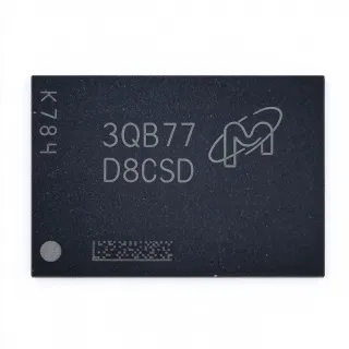
MT53E768M32D2ZW-046 - 24Gbit LPDDR4X SDRAM 200-TFBGA | Micron
MPN: MT53E768M32D2ZW-046 ✓ Active| Qty | Unit Price | Extended |
|---|---|---|
| 1 | $0 | $0.00 |
| 10 | $0 | $0.00 |
| 100 | $0 | $0.00 |
| 500 | $0 | $0.00 |
| 1,000 | $0 | $0.00 |
MT53E768M32D2ZW-046 Overview
LPDDR4X (Low Power Double Data Rate 4X) is a mobile-optimized SDRAM standard derived from the LPDDR4 JEDEC architecture. It belongs to the DRAM -> synchronous dynamic random-access memory -> volatile memory hierarchy and differs from standard DDR4 by using a lower VDDQ core I/O voltage (approximately 0.6V for LPDDR4X versus 1.2V for LPDDR4), which significantly reduces I/O power consumption in battery-operated systems.
Key features include the 24Gbit (3 GB) single-die density, a 32-bit data bus, 3.5 ns clock cycle time, and the WT speed grade supporting 200/264 ball-out configurations. The LVSTL (Low Voltage Swing Termination Logic) interface reduces I/O switching power. A supply voltage range of 1.06V to 1.17V (VDD2) supports low-power operation.
The device is available in commercial WT:C and automotive AAT:C/AIT:C grades, with the automotive variants qualified to AEC-Q100 and rated for operation down to -25C per distributor data. Micron manufactures this part on an advanced DRAM process, using bank-group architecture for high bandwidth efficiency at the 4266 MT/s class data rate of the -046 speed bin.
Typical applications include smartphone and tablet main memory, automotive infotainment and ADAS domain controllers, edge AI compute modules, and embedded industrial systems that pair LPDDR4X with application processors from vendors such as Qualcomm, NXP i.MX, Rockchip, and MediaTek.
Design consideration: LPDDR4X routing requires strict length matching on the 32-bit data bus, controlled impedance, and careful VDDQ decoupling; the Z ball-out requires a specific controller ball-map match, so verify your SoC memory controller supports the Z-die option before layout.
This page synthesizes distributor pricing, same-package drop-in grade variants, design notes, and comparison data not found in the manufacturer datasheet.
Drop-in alternatives for MT53E768M32D2ZW-046 — same package, pin-to-pin compatible. Different-package parts requiring PCB rework are excluded.
Quick Comparison Tool — Select alternative parts for side-by-side comparison:
MT53E768M32D2ZW-046 AAT:C
✅ Drop-In📋 Reference alternative (not in catalog)
MT53E768M32D2ZW-046 AIT:C
✅ Drop-In📋 Reference alternative (not in catalog)
MT53E768M32D2ZW-046 AUT:C
✅ Drop-In📋 Reference alternative (not in catalog)
MT53E768M32D2ZW-046 WT ES:C
✅ Drop-In📋 Reference alternative (not in catalog)
MT53E768M32D2ZW-046 Maximum Ratings & Electrical Characteristics
| Memory Type | Mobile LPDDR4X SDRAM |
| Memory Capacity | 24 Gbit (3 GB) |
| Organization | 768M x 32 |
| Data Rate | 2.133 GHz (4266 MT/s class) |
| Clock Cycle Time | 3.5 ns |
| Interface | LVSTL |
| Supply Voltage Range | 1.06 V to 1.17 V (VDD2) |
| Package | 200-TFBGA (10 x 14.5 mm) |
| Ball Count / Configuration | 200 balls (200/264 option) |
| Speed Grade | -046 |
| Mounting Type | Surface Mount |
| Automotive Qualification | AEC-Q100 (AAT:C / AIT:C grades) |
| Application Grade | WT (commercial/industrial) |
| Bus Width | 32-bit |
| Memory Category Hierarchy | DRAM > SDRAM > Mobile LPDDR4X |
MT53E768M32D2ZW-046 200-tfbga (10 x 14.5 mm) Pin Configuration Guide
Pin configuration for MT53E768M32D2ZW-046 (200-tfbga (10 x 14.5 mm) package). This digital IC includes GPIO, communication interfaces (UART, SPI, I2C), and power pins. Refer to the manufacturer datasheet for alternate pin functions and configuration options. Essential for embedded system design and PCB layout.

No detailed pinout data available for MT53E768M32D2ZW-046.
Refer to the datasheet for full pin configuration.
Typical Applications
MT53E768M32D2ZW-046 is suitable for 6 applications: Smartphone and Tablet Main Memory, Automotive Infotainment and ADAS Domain Controllers, Edge AI Compute Modules, Industrial HMI and Embedded Computing, Networking and Router Appliances, Test and Measurement Instruments.
Smartphone and Tablet Main Memory
The MT53E768M32D2ZW-046 provides 3 GB of LPDDR4X main memory for mid-to-high-tier smartphones and tablets where its 24Gbit single-die density minimizes component count and its LPDDR4X VDDQ (about 0.6V) cuts I/O power versus LPDDR4. Mounted in the 200-ball TFBGA (10 x 14.5 mm) footprint, it pairs directly with Qualcomm Snapdragon and MediaTek Dimensity application processors that support a 32-bit LPDDR4X bus at 2.133 GHz. The 3.5 ns cycle time sustains burst throughput for multitasking UI rendering. Because the package is single-channel 32-bit, designs needing wider bandwidth stack or pair packages; consider the 64-bit MT53E768M64D4HJ-046 for dual-channel SoCs.
Recommended
Automotive Infotainment and ADAS Domain Controllers
For automotive cockpit, infotainment, and ADAS domain controllers, the AEC-Q100-qualified MT53E768M32D2ZW-046 AAT:C / AIT:C grades of this same die deliver 3 GB LPDDR4X with automotive-grade reliability. The 2.133 GHz LVSTL interface sustains the bandwidth demanded by navigation map rendering, camera-surround view stitching, and driver-monitoring pipelines, while the 1.06V to 1.17V supply keeps power budgets aligned with AEC power-tree requirements. Designers must use the automotive suffix parts in vehicles; the WT:C commercial grade does not carry AEC-Q100 qualification. Ball-map compatibility across grades lets one PCB serve both consumer and automotive build options.
Recommended
Edge AI Compute Modules
Edge AI accelerators and SoM (system-on-module) designs use the MT53E768M32D2ZW-046 as on-module DDR memory for neural network inference, where 3 GB of LPDDR4X holds quantized model weights and activation buffers. The 24Gbit density at 768M x 32 matches 32-bit memory controllers on NPU-centric SoCs (Rockchip, Amlogic class), and the 2.133 GHz data rate feeds peak bandwidth during convolution workloads. LPDDR4X self-refresh keeps standby power low for always-on vision applications. Layout on dense SoMs requires the 200-ball footprint plus length-matched fly-by or point-to-point routing per the Micron LPDDR4X system design guide.
Recommended
Industrial HMI and Embedded Computing
Industrial human-machine interfaces and embedded computers deploy the MT53E768M32D2ZW-046 WT:C to run Linux or RTOS stacks with graphical dashboards, where 3 GB of LPDDR4X provides headroom for framebuffers and application memory. The WT industrial grade and the -046 speed bin give stable operation in factory environments, and the 200-TFBGA package withstands vibration better than socketed alternatives. The 1.06V to 1.17V rail simplifies integration with low-voltage PMICs from companion power devices. For harsh extended-temperature sites, switch to the AIT:C automotive-industrial grade without PCB change.
Recommended
Networking and Router Appliances
Wi-Fi 6/7 access points, mesh routers, and SMB gateways use the MT53E768M32D2ZW-046 as main memory alongside network processors, where its 24Gbit capacity buffers packet queues, NAT tables, and management firmware. The 2.133 GHz data rate keeps memory bandwidth from bottlenecking multi-gigabit forwarding, and LPDDR4X power levels suit fanless enclosures that rely on passive cooling. The 200-ball TFBGA (10 x 14.5 mm) footprint integrates into router mainboards with standard reflow assembly. Designs requiring wider bandwidth for multi-core NPUs can migrate to the 64-bit HJ-package family on the same LPDDR4X protocol.
Recommended
Test and Measurement Instruments
Portable oscilloscopes, logic analyzers, and spectrum analyzers use the MT53E768M32D2ZW-046 to capture and buffer high-speed waveform data, where 3 GB of LPDDR4X extends record length for deep-memory acquisitions. The 2.133 GHz burst rate matches the sustained write bandwidth needed for streaming ADC data into memory, while low LPDDR4X I/O power reduces thermal load inside sealed instrument housings. The engineering-sample MT53E768M32D2ZW-046 WT ES:C supports early firmware bring-up of memory controllers before production silicon is committed. Bench and field instruments alike benefit from the vibration-tolerant 200-ball TFBGA mount.
Recommended
Recommended Products Summary
Engineering reference data for MT53E768M32D2ZW-046 — comparison, design guidance, and compliance information.
Selection Guide
Comparison with Alternatives
| Parameter | This Product | MT53E768M32D2ZW-046 AAT:C | MT53E768M32D2ZW-046 AIT:C | MT53E768M32D2ZW-046 AUT:C |
|---|---|---|---|---|
| Package | 200-TFBGA (10 x 14.5 mm) | 200-TFBGA (10 x 14.5 mm) - same | 200-TFBGA (10 x 14.5 mm) - same | 200-TFBGA (10 x 14.5 mm) - same |
| Brand | Micron Technology | Micron Technology | Micron Technology | Micron Technology |
| Memory Capacity | 24 Gbit (3 GB) | 24 Gbit (3 GB) | 24 Gbit (3 GB) | 24 Gbit (3 GB) |
| Organization | 768M x 32 | 768M x 32 | 768M x 32 | 768M x 32 |
| Data Rate | 2.133 GHz (3.5 ns) | 2.133 GHz (3.5 ns) | 2.133 GHz (3.5 ns) | 2.133 GHz (3.5 ns) |
| Interface | LVSTL (LPDDR4X) | LVSTL (LPDDR4X) | LVSTL (LPDDR4X) | LVSTL (LPDDR4X) |
| AEC-Q100 Qualification | No (commercial/industrial WT grade) | Yes (automotive) | Yes (automotive-industrial) | Yes (automotive) |
| Supply Voltage (VDD2) | 1.06 V to 1.17 V | 1.06 V to 1.17 V | 1.06 V to 1.17 V | 1.06 V to 1.17 V |
| Distributor Availability (as of 2026-09-04) | In stock at DigiKey/Mouser/Newark (WT:C, TR) | In stock at DigiKey | In stock at DigiKey | Zero stock; factory lead time |
Key Differentiators
- 24Gbit single-die density in a compact 200-ball footprint (vs MT53E256M16D1FW-046)
- LPDDR4X VDDQ power advantage (vs MT53D512M32D2NP-046 (LPDDR4-class power profile))
- AEC-Q100 automotive grade variants available pin-to-pin (vs MT53E768M32D2ZW-046 AAT:C)
Design Notes
LPDDR4X at 2.133 GHz demands tight fly-by or point-to-point routing on all 32 data bits plus DQS strobes. Keep trace-length skew within the SoC memory controller spec (typically a few tens of mils per 100 mm class), reference solid ground planes, and impedance-control to 40-50 ohm single-ended. Follow the Micron LPDDR4X system design guide for Z-ballout stub control; the 200-ball TFBGA allows short fanout vias that minimize stub reflection.
Provide separate, tightly regulated rails for VDD2 (1.06V to 1.17V) and the LPDDR4X VDDQ domain (approximately 0.6V). Place bulk and high-frequency ceramic decoupling directly under the 200-TFBGA footprint using via-in-pad arrays. Confirm the PMIC supports LPDDR4X VDDQ-switching for self-refresh power savings. Verify the VDD2 rail tolerance under full-bandwidth burst conditions, where peak current transients exceed idle levels by a large factor.
Verify that your SoC memory controller supports the Z ball-out option and includes -046 (2.133 GHz) memory-training tables in firmware; many LPDDR4X controllers only support specific die options and speed bins. Also confirm the grade suffix in production: automotive builds must order AAT:C or AIT:C (AEC-Q100), not WT:C. The ES:C engineering-sample part must never be shipped in production units.
Compliance Information
This WT:C grade is not AEC-Q100 qualified; automotive AAT:C/AIT:C grades are qualified per distributor data. RoHS/REACH status must be confirmed on the Micron part-detail page.