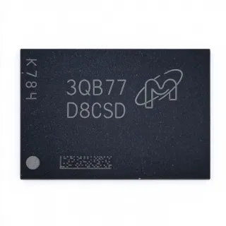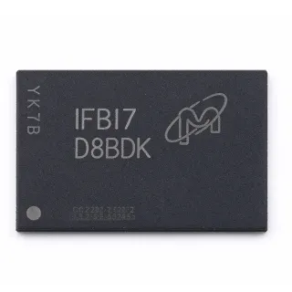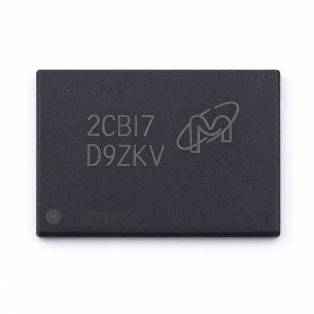
MT53E256M32D2FW-046 - 8Gbit LPDDR4X 2133MHz TFBGA | Micron
MPN: MT53E256M32D2FW-046 ✓ Active| Qty | Unit Price | Extended |
|---|---|---|
| 1 | $19.4063 | $19.41 |
| 10 | $14.0156 | $140.16 |
| 100 | $12.3984 | $1,239.84 |
| 500 | $11.8594 | $5,929.70 |
| 1,000 | $11.3203 | $11,320.30 |
MT53E256M32D2FW-046 Overview
LPDDR4X (Low Power Double Data Rate 4X) is a member of the JEDEC-defined LPDDR (Low Power Double Data Rate) SDRAM family - a voltage-reduced evolution of LPDDR4 optimized for mobile and battery-powered systems. Within the memory hierarchy, LPDDR4X sits alongside LPDDR4 as a low-power DRAM alternative to DDR4 and GDDR types, prioritizing bandwidth-per-watt over absolute peak bandwidth. LPDDR4X reduces the I/O termination voltage relative to LPDDR4, lowering overall power consumption in memory-active workloads.
Key features of this device include the 256M x 32 organization that simplifies 32-bit memory bus designs, a 2133 MHz (2.133 GHz) data rate for high-throughput SoC interfaces, and low-power operation modes suited to battery-powered platforms. Per Micron product documentation, family features include auto self-refresh with a built-in temperature sensor, auto precharge, write leveling, and ZQ calibration functions.
The dual-die package architecture balances density and cost: two dies share the package ball map while the memory controller addresses them as a single logical bank group set, enabling high density without enlarging the PCB footprint. The 200-TFBGA (10 x 14.5 mm) package is a standard footprint shared across the MT53E256M32D2 and MT53E512M32D2 families, supporting PCB reuse when densities change.
Typical applications include smartphone and tablet DRAM, embedded vision and camera modules, automotive infotainment SoC memory, and industrial edge-AI platforms that use LPDDR4X memory controllers. The -046 speed grade (3.5 ns access time) aligns with common mobile SoC memory controller timing budgets.
When designing with this device, route the LPDDR4X fly-by command/address bus with length-matched stubs and verify controller firmware timing parameters against the -046 speed bin, because LPDDR4X training and termination settings differ from LPDDR4.
This page synthesizes distributor pricing, drop-in alternatives, and practical design notes not found in the manufacturer datasheet.
Drop-in alternatives for MT53E256M32D2FW-046 — same package, pin-to-pin compatible. Different-package parts requiring PCB rework are excluded.
Quick Comparison Tool — Select alternative parts for side-by-side comparison:
MT53E512M32D2FW-046 AAT:D
✓ In Stock
$13.75 / Unit
View Datasheet →MT53E256M32D2FW-046 IT:B
📋 Reference alternative (not in catalog)
MT53E256M32D2FW-046 AUT:B
📋 Reference alternative (not in catalog)
MT53E256M32D2FW-046 AAT:B
📋 Reference alternative (not in catalog)
MT53E256M32D2FW-046 AIT:B
📋 Reference alternative (not in catalog)
MT53E256M32D2FW-046 Maximum Ratings & Electrical Characteristics
| Memory Type | SDRAM - Mobile LPDDR4X |
| Memory Size | 8 Gbit |
| Organization | 256M x 32 |
| Interface | Parallel |
| Clock Frequency | 2.133 GHz |
| Access Time | 3.5 ns |
| Speed Grade | -046 |
| Package | 200-TFBGA (10 x 14.5 mm) |
| Die Configuration | Dual Die Package (DDP) |
| Mounting Type | Surface Mount |
| Auto Self-Refresh | Yes (with built-in temperature sensor) |
| Write Leveling | Yes |
| ZQ Calibration | Yes |
| Auto Precharge | Yes |
MT53E256M32D2FW-046 200-tfbga (10 x 14.5 mm) Pin Configuration Guide
Pin configuration for MT53E256M32D2FW-046 (200-tfbga (10 x 14.5 mm) package). This digital IC includes GPIO, communication interfaces (UART, SPI, I2C), and power pins. Refer to the manufacturer datasheet for alternate pin functions and configuration options. Essential for embedded system design and PCB layout.

No detailed pinout data available for MT53E256M32D2FW-046.
Refer to the datasheet for full pin configuration.
Typical Applications
MT53E256M32D2FW-046 is suitable for 6 applications: Smartphone and Tablet Main Memory, Automotive Infotainment and Cluster, Embedded Vision and Camera Modules, Industrial Edge-AI Gateways, Battery-Powered Portable Instruments, Networking and Edge Router Buffering.
Smartphone and Tablet Main Memory
The MT53E256M32D2FW-046 fits smartphone and tablet main-memory designs that require 8 Gbit of LPDDR4X on a 32-bit parallel bus. Its 2.133 GHz data rate matches mainstream mobile SoC memory controllers, while the 3.5 ns access time (-046 speed grade) meets standard mobile timing budgets. LPDDR4X technology lowers I/O termination voltage relative to LPDDR4, and the built-in temperature sensor with auto self-refresh trims refresh power in standby - a major share of idle drain. The dual-die (DDP) 200-TFBGA (10 x 14.5 mm) footprint supports compact stacked logic-plus-memory layouts common in handset PCBs.
Recommended
Automotive Infotainment and Cluster
For automotive infotainment and digital cockpit platforms, select the MT53E256M32D2FW-046 AUT:B or AAT:B automotive grade. Micron publishes a dedicated MT53E256M32D2 automotive LPDDR4/LPDDR4X datasheet, and Mouser and Avnet stock the AUT variant. The 8 Gbit capacity comfortably supports navigation maps, media buffering, and HMI frame buffers, while the 256M x 32 organization pairs naturally with 32-bit automotive SoC memory buses. Automotive grade temperature rating addresses cabin thermal environments; the identical 200-TFBGA footprint means an industrial or commercial prototype can be migrated to the automotive grade with no PCB change.
Recommended
Embedded Vision and Camera Modules
Embedded vision SoCs that stream multiple image sensors need DRAM bandwidth for line buffering, ISP frame processing, and ISP-to-encoder handoff. The MT53E256M32D2FW-046's 2133 MHz parallel interface supplies that bandwidth at low power, and the built-in temperature sensor allows the memory to adapt self-refresh behavior in sealed camera housings that run warm. The 8 Gbit density suits 1080p30 multi-camera edge platforms with object-detection workloads. Use the industrial IT:B grade for -40C to +95C ambient environments such as outdoor or vehicle-mounted cameras, per LCSC's specification of the AIT:B variant.
Recommended
Industrial Edge-AI Gateways
Industrial edge-AI gateways running inference on sensor streams use LPDDR4X for model weights and activation buffers. The MT53E256M32D2FW-046 provides 8 Gbit with 2.133 GHz bandwidth, enough for quantized CNN inference workloads, while the IT:B grade's -40C to +95C rating (confirmed on LCSC for the AIT:B) covers unconditioned cabinets. ZQ calibration maintains signal integrity over temperature drift, and write leveling eases fly-by routing in dense gateway boards. The standard 200-TFBGA footprint is widely supported by LPDDR4X controller reference designs, shortening firmware bring-up for industrial platforms.
Recommended
Battery-Powered Portable Instruments
Handheld test instruments, medical monitors, and portable data loggers benefit from the LPDDR4X power profile of the MT53E256M32D2FW-046. Auto self-refresh with the internal temperature sensor reduces refresh frequency at low ambient temperatures, cutting memory standby current - often a dominant contributor to instrument sleep-mode draw. The parallel 32-bit interface and 3.5 ns access time sustain UI rendering and data logging without imposing high idle current. Micron family features including auto precharge simplify controller configuration for always-on logging firmware in battery-constrained designs.
Recommended
Networking and Edge Router Buffering
Edge networking equipment and compact router platforms use LPDDR4X DRAM for packet buffering, route tables, and management-plane software. The MT53E256M32D2FW-046's 8 Gbit capacity and 2133 MHz interface support gigabit-class throughput with headroom for burst absorption, while the 256M x 32 organization maps efficiently to 32-bit memory controller buses common in networking SoCs. The commercial WT grade suits office-environment equipment; the IT:B variant extends rating to -40C to +95C for outdoor enclosures. The standard TFBGA footprint allows buffer-memory capacity upgrades within the same footprint family when traffic profiles grow.
Recommended
Recommended Products Summary
Engineering reference data for MT53E256M32D2FW-046 — comparison, design guidance, and compliance information.
Selection Guide
Comparison with Alternatives
| Parameter | This Product | MT53E256M32D2FW-046 IT | MT53E256M32D2FW-046 AUT | MT53E256M32D2FW-046 AAT | MT53E256M32D2FW-046 AIT | MT53E512M32D2FW-046 AAT |
|---|---|---|---|---|---|---|
| Package | 200-TFBGA (10 x 14.5 mm) | B: 200-TFBGA (10 x 14.5 mm) - same | B: 200-TFBGA (10 x 14.5 mm) - same | B: 200-TFBGA (10 x 14.5 mm) - same | B: 200-TFBGA (10 x 14.5 mm) - same | D: 200-TFBGA (10 x 14.5 mm) - same footprint family |
| Brand | Micron Technology | B: Micron Technology | B: Micron Technology | B: Micron Technology | B: Micron Technology | D: Micron Technology |
| Memory Density | 8 Gbit | B: 8 Gbit | B: 8 Gbit | B: 8 Gbit | B: 8 Gbit | D: 16 Gbit (+100%) |
| Organization | 256M x 32 | B: 256M x 32 | B: 256M x 32 | B: 256M x 32 | B: 256M x 32 | D: 512M x 32 |
| Access Time | 3.5 ns (-046) | B: 3.5 ns (-046) | B: 3.5 ns (-046) | B: 3.5 ns (-046) | B: 3.5 ns (-046) | D: 3.5 ns (-046) |
| Technology | LPDDR4X (DDP) | B: LPDDR4X (DDP) | B: LPDDR4 (per Mouser listing) | B: LPDDR4X | B: LPDDR4X | D: LPDDR4X |
| Grade / Qualification | Commercial (WT) | B: Industrial (IT) | B: Automotive (AUT) | B: Automotive (AAT) | B: Automotive Industrial (AIT) | D: Automotive (AAT) |
Key Differentiators
- LPDDR4X reduced-termination-voltage power profile (vs MT53E256M32D2FW-046 AUT:B)
- Dual-die density scaling in fixed footprint (vs MT53E512M32D2FW-046 AAT:D)
- Extended-temperature drop-in availability (vs MT53E256M32D2FW-046 IT:B)
Design Notes
At the 2133 MHz data rate of the -046 speed grade, LPDDR4X data-group routing demands controlled impedance (~50 ohm single-ended, ~100 ohm differential), reference-plane continuity at layer transitions, and intra-byte length matching to a fraction of the unit interval. Use fly-by topology for command/address with calibrated per-die training, since the DDP construction exposes two dies. Follow the LPDDR4X reference layout in the memory controller vendor's design guide and run SI simulation on the length-matched net groups before tape-out.
LPDDR4X uses reduced I/O termination voltage, so verify that the SoC memory controller supports LPDDR4X termination levels - substituting an LPDDR4 part or controller mismatch changes the termination power budget. Decouple the core and I/O supply rails with the capacitor network specified in the Micron datasheet reference design, placing bulk capacitance near the TFBGA ball assignments. Estimated: at multi-hundred-milliwatt active levels, rail ripple above the LPDDR4X spec window can cause read-eye degradation at 2.133 GHz, so measure supply noise at the balls during bring-up.
The FW suffix indicates a dual-die package (DDP): the controller must support the two-die address mapping and execute training per die. A firmware timing table written for a single-die LPDDR4 part will not initialize correctly. Also match the grade suffix to your environment - the WT commercial grade is not qualified for automotive temperature, so production automotive builds must move to the AUT:B/AAT:B variant (same footprint, no PCB change). Finally, enter the -046 speed bin parameters into the controller, not generic LPDDR4 defaults.
The 200-TFBGA (10 x 14.5 mm) ball map concentrates high-speed DQ groups on the package perimeter; plan the stack-up so each data byte group has an adjacent reference plane and route on the layer closest to that plane. Micron provides CAD footprints and 3D models via componentsearchengine.com for this MPN - use the vendor footprint rather than a generic 200-ball pattern, because ball pitch and die-pad thermal relief differ between Micron FW-family variants.
Compliance Information
Compliance status was not stated in the retrieved web data. Automotive grade variants (AUT/AAT/AIT) exist per Mouser/Avnet/Micron listings; consult the Micron part-detail page and product environmental datasheets for current RoHS/REACH declarations.