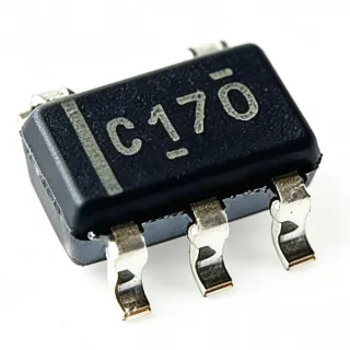
SN74LVC1G08DBVR - 2-Input AND Gate 1.65-5.5V | TI
MPN: SN74LVC1G08DBVR ✓ Active| Qty | Unit Price | Extended |
|---|---|---|
| 1 | $0.32 | $0.32 |
| 10 | $0.24 | $2.40 |
| 100 | $0.13 | $13.00 |
| 500 | $0.08 | $40.00 |
| 1,000 | $0.058 | $58.00 |
| 3,000 | $0.036 | $108.00 |
SN74LVC1G08DBVR Overview
A logic gate is a fundamental building block of digital electronics that performs a Boolean operation on binary inputs to produce a single binary output. An AND gate outputs HIGH only when all inputs are HIGH. Single-gate logic (little logic) places one gate in a small package, letting designers add glue logic to dense boards without dedicating a full multi-gate IC. The SN74LVC1G08 belongs to the LVC (Low-Voltage CMOS) logic family within the broader 74-series logic hierarchy.
Key features include 5-V tolerant inputs regardless of VCC, a typical propagation delay (tpd) of 3.3 ns at 3.3 V, and low power consumption with 10 uA maximum ICC. The Ioff feature supports partial-power-down operation, blocking backdrive current when VCC is removed - essential for multi-rail systems.
Technically, the device uses CMOS technology for high noise immunity and low static power dissipation. TI provides a controlled baseline with one assembly/test site and one fabrication site for consistent quality. The SOT-23-5 footprint is universally supported by PCB tools, and the family also offers the ultra-small 0.64 mm2 DPW package with 0.5 mm pitch for space-critical designs.
Typical applications include signal gating, enable/disable logic, clock gating, and 3.3 V to 5 V interfacing in portable electronics, industrial control, and communication equipment. The wide supply range and robust 32 mA drive make it ideal for mixed-voltage glue logic.
Design tip: decouple VCC with a 0.1 uF ceramic capacitor close to the device and tie unused inputs to a defined logic level - floating CMOS inputs can oscillate and draw excess current. Pricing references are as of 2026-08-30.
Drop-in alternatives for SN74LVC1G08DBVR — same package, pin-to-pin compatible. Different-package parts requiring PCB rework are excluded.
Variants in this series
Same-series models that are drop-in compatible with SN74LVC1G08DBVR (same form factor and footprint) — differing in RoHS Status, Logic Family, Logic Function, Number of Gates, Operating Temperature.
Quick Comparison Tool — Select alternative parts for side-by-side comparison:
SN74AHC1G08QDCKRQ1
✅ Drop-In✓ In Stock
$0.09 / Unit
View Datasheet →SN74LVC1G08DRLR
⚡ Same Package📋 Reference alternative (not in catalog)
SN74LVC1G08DPWR
⚡ Same Package📋 Reference alternative (not in catalog)
74LVC1G08GW,125
✅ Drop-In ⚠️ Specs Unverified📋 Reference alternative (not in catalog)
74LVC1G08SE-7
✅ Drop-In ⚠️ Specs Unverified📋 Reference alternative (not in catalog)
NC7SZ08M5X
✅ Drop-In ⚠️ Specs Unverified📋 Reference alternative (not in catalog)
SN74LVC1G08DBVR Maximum Ratings & Electrical Characteristics
| Logic Function | AND Gate |
| Circuits per Package | 1 |
| Inputs per Gate | 2 |
| Supply Voltage Range | 1.65 V to 5.5 V |
| Output Drive | 32 mA at 3.3 V |
| Propagation Delay (tpd) | 3.3 ns typical at 3.3 V |
| Max Quiescent Current (ICC) | 10 uA |
| Input Tolerance | 5.5 V regardless of VCC |
| Ioff (Partial Power Down) | Yes |
| Logic Family | LVC (Low-Voltage CMOS) |
| Technology | CMOS |
| Package | SOT-23-5 (DBV) |
| Mounting Type | Surface Mount |
| Operating Temperature | -40C to +125C |
| RoHS Status | Compliant |
| Output Type | Push-Pull |
SN74LVC1G08DBVR Pin Configuration
| Pin 1 | A — Input A |
| Pin 2 | B — Input B |
| Pin 3 | GND — Ground |
| Pin 4 | Y — Output (Y = A AND B, positive logic) |
| Pin 5 | VCC — Power supply, 1.65 V to 5.5 V |
Typical Applications
SN74LVC1G08DBVR is suitable for 6 applications: Signal Gating and Enable Logic, Clock Gating for Low Power, 3.3 V to 5 V Logic Interfacing, Portable and Battery-Powered Electronics, Industrial Control Interlocks, Automotive Electronic Control Units.
Signal Gating and Enable Logic
The SN74LVC1G08DBVR gates a signal with an enable so the output passes only when both conditions are true - the fundamental AND use case. Its 3.3 ns typical propagation delay at 3.3 V keeps added timing skew small in control paths, while the 32 mA drive directly drives LEDs, optocouplers or fanout loads. Use it between an MCU GPIO and peripheral chip-select lines to enforce hard enable conditions in industrial control boards.
Recommended
Clock Gating for Low Power
ANDing a clock with a power-down control bit stops clock distribution to idle blocks, cutting dynamic power in battery-operated designs. The SN74LVC1G08DBVR adds only ~3.3 ns typical delay at 3.3 V and 10 uA maximum ICC, negligible versus system power savings. Because CMOS inputs must not float when gating, tie the inactive path to a defined level; decouple VCC with 0.1 uF to suppress glitching during enable transitions.
Recommended
3.3 V to 5 V Logic Interfacing
Because inputs tolerate up to 5.5 V regardless of VCC, a 3.3 V-supplied SN74LVC1G08DBVR can accept 5 V logic inputs and drive downstream logic at its own VCC level, forming a safe mixed-voltage interface point. This suits bridging legacy 5 V peripherals to modern 3.3 V MCUs. Push-pull CMOS output eliminates pull-up resistors needed by open-drain solutions, and the SOT-23-5 footprint keeps the interface compact on crowded boards.
Recommended
Portable and Battery-Powered Electronics
With 10 uA maximum quiescent current, 1.65 V operation and the tiny SOT-23-5 outline, the SN74LVC1G08DBVR fits power- and space-constrained portable products such as wearables and hand-held instruments. The Ioff feature prevents backdrive current when VCC is removed during partial power-down, protecting multi-rail battery designs. Its wide supply range lets one BOM line serve 1.8 V, 2.5 V, 3.3 V and 5 V product variants.
Recommended
Industrial Control Interlocks
Safety interlock logic often requires an output to be true only when multiple conditions are met - door closed, guard engaged, power present. The SN74LVC1G08DBVR implements this in a single 2-input gate with -40C to +125C operation for harsh factory environments and CMOS noise immunity for electrically noisy panels. Its 32 mA output can directly drive indicator LEDs or optocoupler inputs for PLC-level signaling without additional buffer stages.
Recommended
Automotive Electronic Control Units
In 12 V automotive ECUs translated to 5 V logic domains, the SN74LVC1G08DBVR performs combination gating of sensor flags and enable signals. Its 5.5 V tolerant inputs survive transients on 5 V rails, and the wide -40C to +125C temperature range matches under-hood adjacent cabin electronics. For new AEC-Q100 designs requiring automotive qualification, pair it with the TI Q1 single-gate family such as SN74LVC1G08 Q1 variants for full compliance.
Recommended
Recommended Products Summary
Engineering reference data for SN74LVC1G08DBVR — comparison, design guidance, and compliance information.
Selection Guide
Comparison with Alternatives
| Parameter | This Product | SN74AHC1G08QDCKRQ1 | 74LVC1G08GW,125 | 74LVC1G08SE-7 | NC7SZ08M5X |
|---|---|---|---|---|---|
| Package | SOT-23-5 (DBV) | SC70-5 (DCK) | SOT-23-5 - same | SOT-23-5 - same | SOT-23-5 - same |
| Brand | Texas Instruments | Texas Instruments | NXP Semiconductors | Diodes Incorporated | onsemi |
| Logic Function | 2-input AND | 2-input AND | 2-input AND | 2-input AND | 2-input AND |
| Automotive Grade | No | Yes (AEC-Q100 Q1) | No | No | No |
Key Differentiators
- Widest supply range in single-gate AND family (vs NC7SZ08M5X)
- 5.5 V overvoltage-tolerant inputs regardless of VCC (vs NC7SZ08M5X)
- Controlled baseline manufacturing (vs 74LVC1G08SE-7)
Design Notes
Decouple VCC with a 0.1 uF ceramic capacitor placed within 2-3 mm of the SOT-23-5 VCC pin. Single-gate logic in small packages is sensitive to supply droop during fast output transitions; a good decoupling network prevents output glitches when driving 32 mA loads. The SOT-23-5 land pattern is standard in all PCB CAD libraries - no special footprint work is needed.
Never leave A or B inputs floating on CMOS devices - floating inputs can oscillate and draw excess current beyond the 10 uA ICC spec. Tie unused logic to GND (for AND, an unused input at GND forces output LOW) or drive it from a defined logic level. When gating clocks, ensure the gating signal changes state only while the clock is LOW to avoid runt pulses.
The Ioff feature allows safe partial-power-down: inputs up to 5.5 V will not backdrive a removed VCC rail. However, verify current paths in multi-rail designs - if another rail drives this gate's inputs while VCC is off, Ioff limits leakage but the output is undefined. Add a pulldown on the output if downstream loads must remain LOW during power sequencing.
At 3.3 ns typical propagation delay, keep traces short (under 10 cm at moderate edge rates) or add series termination for long lines. The push-pull CMOS output with 32 mA drive creates fast edges; series resistors of 22-33 ohm at the output reduce reflections on longer traces without significantly increasing delay.
Compliance Information
RoHS compliant per TI product page and DigiKey listing. For AEC-Q100 qualified version use SN74LVC1G08 Q1 variants.