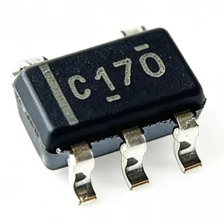
SN74AHC1G00DBVR - 2-5.5V Single 2-Input NAND Gate | Texas Instruments
MPN: SN74AHC1G00DBVR ✓ Active| Qty | Unit Price | Extended |
|---|---|---|
| 1 | $0.29 | $0.29 |
| 10 | $0.22 | $2.20 |
| 100 | $0.14 | $14.00 |
| 500 | $0.1 | $50.00 |
| 1,000 | $0.07 | $70.00 |
SN74AHC1G00DBVR Overview
A NAND gate is a fundamental digital logic gate that outputs LOW only when all inputs are HIGH. It is a universal gate, meaning any other logic function (AND, OR, NOT, XOR) can be built from NAND gates alone. The SN74AHC1G00 belongs to the AHC (Advanced High-Speed CMOS) logic family, which balances speed and power for battery-powered and portable systems within the broader CMOS logic IC hierarchy.
Key features include a wide 2-V to 5.5-V operating range, a maximum propagation delay of 6.5 ns at 5 V, and maximum quiescent supply current of only 10 uA. Schmitt-trigger action on all inputs provides hysteresis-based noise immunity, allowing slow input edges without false triggering and eliminating external conditioning components. The device delivers ±8 mA output drive at 5 V, compatible with standard CMOS and TTL logic levels.
Fabricated in advanced CMOS technology, the SN74AHC1G00 combines high-speed switching with low static and dynamic power dissipation. Robustness features include latch-up performance exceeding 250 mA per JESD 17 and ESD protection exceeding 2000-V HBM, 200-V MM, and 1000-V CDM ratings per the TI datasheet.
Typical applications include signal gating, logic inversion, clock gating, and interface buffering in consumer electronics, industrial control, and automotive subsystems. The small SOT-23-5 footprint suits wearables, IoT modules, and dense PCBs where board area is at a premium.
Design tip: do not let input voltages exceed VCC, and decouple the VCC pin with a 0.1-uF ceramic capacitor for best noise performance. Pricing shown reflects distributor data as of 2026-08-29.
Drop-in alternatives for SN74AHC1G00DBVR — same package, pin-to-pin compatible. Different-package parts requiring PCB rework are excluded.
Variants in this series
Same-series models that are drop-in compatible with SN74AHC1G00DBVR (same form factor and footprint) — differing in Logic Family, Package, Operating Temperature, Supply Voltage (VCC), Input Type.
Quick Comparison Tool — Select alternative parts for side-by-side comparison:
SN74LVC1G00DBVR
✅ Drop-In📋 Reference alternative (not in catalog)
SN74AHC1G86DBVR
⚡ Same Package📋 Reference alternative (not in catalog)
NC7SZ00M5X
✅ Drop-In ⚠️ Specs Unverified✓ In Stock
$0.07 / Unit
View Datasheet →NC7S00M5X
✅ Drop-In✓ In Stock
$0.1 / Unit
View Datasheet →74LVC1G00GW
✅ Drop-In ⚠️ Specs Unverified✓ In Stock
$0.035 / Unit
View Datasheet →74VHC1G00
✅ Drop-In ⚠️ Specs Unverified📋 Reference alternative (not in catalog)
SN74AHC1G00DBVR Maximum Ratings & Electrical Characteristics
| Logic Function | 2-Input Positive-NAND Gate |
| Supply Voltage Range | 2 V to 5.5 V |
| Max Propagation Delay | 6.5 ns at 5 V |
| Quiescent Current (Max ICC) | 10 uA |
| Output Drive | ±8 mA at 5 V |
| Input Type | Schmitt Trigger (all inputs) |
| Latch-Up Performance | Exceeds 250 mA per JESD 17 |
| ESD Protection HBM | Exceeds 2000 V |
| ESD Protection MM | Exceeds 200 V |
| ESD Protection CDM | Exceeds 1000 V |
| Logic Family | AHC (Advanced High-Speed CMOS) |
| Package | SOT-23-5 (DBV) |
| Mounting Type | Surface Mount |
| Number of Channels | 1 |
| RoHS Status | Compliant |
SN74AHC1G00DBVR Pin Configuration
| Pin 1 | A — Input A |
| Pin 2 | GND — Ground |
| Pin 3 | B — Input B |
| Pin 4 | Y — Output (Y = NOT(A AND B) in positive logic) |
| Pin 5 | VCC — Power supply, 2 V to 5.5 V |
Typical Applications
SN74AHC1G00DBVR is suitable for 6 applications: Signal Gating in Industrial Control, IoT and Wearable Modules, Clock Gating and Power Management, Automotive Subsystems (5-V Logic Glue), Logic Level Combination in Consumer Electronics, Test and Measurement Interface Boards.
Signal Gating in Industrial Control
In industrial control boards, the SN74AHC1G00 gates sensor enable lines and interlock signals where noise immunity is critical. The Schmitt-trigger inputs tolerate slow edges from optocouplers and RC-filtered sensor outputs without false switching, while the 2-5.5 V range supports both legacy 5-V and 3.3-V PLC logic rails. The ±8 mA output drive at 5 V can directly drive LED indicators or optocoupler inputs, and the 10 uA max quiescent current keeps standby power low in always-on monitoring equipment.
Recommended
IoT and Wearable Modules
Battery-powered IoT nodes and wearables benefit from the SN74AHC1G00's 10 uA maximum ICC and tiny SOT-23-5 footprint of roughly 2.9 x 2.8 mm. It handles wake-up logic, button debouncing assisted by Schmitt inputs, and power-rail gating between the MCU and sensors. The 2 V minimum supply supports operation from a discharged lithium cell through a regulator down to 2.5 V, and the 6.5 ns propagation delay keeps wake latency negligible. Single-gate packaging minimizes board area in dense sensor-module layouts.
Recommended
Clock Gating and Power Management
The SN74AHC1G00 is widely used to gate clocks to peripherals in power-sensitive systems: one input carries the clock, the other an enable signal, so Y goes HIGH (clock disabled) whenever the enable is LOW. The 6.5 ns max tpd at 5 V limits added clock skew, and Schmitt-trigger inputs clean up slowly ramping enable signals from supervisor ICs or RC power-on circuits. Low dynamic power in the AHC CMOS process keeps gated-clock dissipation negligible compared with the peripheral being switched off.
Recommended
Automotive Subsystems (5-V Logic Glue)
In non-safety automotive modules such as body controllers and sensor hubs, the SN74AHC1G00 provides 5-V glue logic with robust ESD protection exceeding 2000-V HBM and latch-up performance above 250 mA per JESD 17. It gates fault signals, inverts sensor polarities, and combines enable conditions for actuators. For new automotive designs requiring AEC-Q100 qualification, TI offers qualified single-gate logic such as the SN74LVC1G17QDBVRQ1 family within the same small-package ecosystem.
Recommended
Logic Level Combination in Consumer Electronics
Consumer products such as set-top boxes, appliances, and audio accessories use the SN74AHC1G00 to combine push-button, IR-receiver, and microcontroller outputs into a single control signal. Schmitt-trigger inputs accept slow RC-filtered button signals directly, eliminating debounce comparators. The 3.3-V operation matches typical MCU GPIO levels, while the ±8 mA drive can blink a status LED. Its low cost (well under $0.10 in volume as of 2026-08-29) makes single-gate glue logic a trivial BOM addition.
Recommended
Test and Measurement Interface Boards
On test-fixture and instrumentation interface boards, the SN74AHC1G00 combines trigger and arm signals, inverts polarity of instrument outputs, and gates counter/timer inputs. The 6.5 ns max propagation delay at 5 V preserves trigger timing accuracy, and the 2000-V HBM ESD rating helps survive connector-transient exposure during fixture handling. Schmitt-trigger inputs condition slowly rising trigger signals from phototransistor or comparator outputs, ensuring one clean output edge per trigger event on dense patch-panel designs.
Recommended
Recommended Products Summary
Engineering reference data for SN74AHC1G00DBVR — comparison, design guidance, and compliance information.
Selection Guide
Comparison with Alternatives
| Parameter | This Product | SN74LVC1G00DBVR | NC7SZ00M5X | 74LVC1G00GW |
|---|---|---|---|---|
| Package | SOT-23-5 (DBV) | SOT-23-5 (DBV) - same | SOT-23-5 - same | SOT-23-5 - same |
| Brand | Texas Instruments | Texas Instruments | onsemi | Nexperia |
| Supply Voltage Range | 2 V to 5.5 V | 1.65 V to 5.5 V | 1.65 V to 5.5 V | 1.65 V to 5.5 V |
| Logic Function | 2-Input NAND | 2-Input NAND | 2-Input NAND | 2-Input NAND |
| Schmitt Trigger Inputs | Yes | No | No | No |
Key Differentiators
- Schmitt-trigger inputs on all inputs (vs SN74LVC1G00DBVR)
- Wide 2-5.5 V supply range (vs NC7SZ00M5X)
- Robust ESD and latch-up ratings (vs 74LVC1G00GW)
Design Notes
Decouple the VCC pin with a 0.1-uF ceramic capacitor placed within 2 mm of pin 5. During output transitions the CMOS stage draws dynamic shoot-through current; without local decoupling this creates supply bounce that can couple into nearby analog circuitry. The 10 uA static ICC is negligible, but dynamic power scales as C x V^2 x f, so at 5 V and high toggle rates keep trace capacitance low.
Never let an input voltage exceed VCC - the AHC input structure lacks the overvoltage tolerance of the LVC family, and inputs above VCC can forward-bias protection structures and cause latch-up. When translating from a 5-V domain into a 3.3-V-supplied gate, use a level translator such as the SN74LVC1T45DCKR instead of direct connection.
Exploit the Schmitt-trigger inputs: slow edges from optocouplers, RC power-on circuits, or long cables can connect directly without a separate buffer. However, keep PCB traces between a Schmitt input and its source short when in a noisy environment - hysteresis rejects slow noise, not high-frequency ringing near the threshold. Terminate long lines and add a small series resistor (22-33 ohm) at output Y when driving heavy capacitive loads.
Compliance Information
RoHS compliant per TI product page. AEC-Q100 qualification not indicated for this standard part; see TI Q1 single-gate logic for automotive-qualified options.