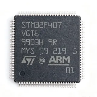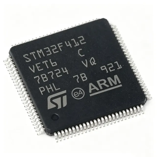
STM32F412VET6 - 512KB Flash ARM Cortex-M4F MCU | STMicroelectronics
MPN: STM32F412VET6 ✓ Active| Qty | Unit Price | Extended |
|---|---|---|
| 1 | $13.6364 | $13.64 |
| 10 | $9.8485 | $98.49 |
| 100 | $8.7121 | $871.21 |
| 500 | $8.3333 | $4,166.65 |
| 1,000 | $7.9545 | $7,954.50 |
STM32F412VET6 Overview
What is a microcontroller? A microcontroller (MCU) is a compact integrated circuit designed to govern a specific operation in an embedded system. It contains a processor core, memory (Flash and SRAM), and programmable input/output peripherals on a single chip. Microcontrollers are the brains of countless electronic devices, from automotive engine control units to IoT sensors and consumer electronics. The STM32F412VET6 belongs to the STM32F4 series, which is part of the broader STM32 family of 32-bit ARM Cortex-M based MCUs, positioned between the value-line STM32F0/F1 series and the high-performance STM32F7/H7 series.
Key features of the STM32F412VET6 include a 100 MHz ARM Cortex-M4F core with DSP instructions and a floating-point unit (FPU), 512 KB of Flash memory, 256 KB of SRAM, and a comprehensive set of peripherals. It offers multiple communication interfaces: 3x I2C, 4x USART, 5x SPI, 2x CAN, 1x SDIO, 1x USB 2.0 OTG FS, and 1x FMC (Flexible Memory Controller) for external memory expansion. The device also includes a 12-bit ADC with up to 16 channels, a 12-bit DAC, advanced timers, and a true random number generator (TRNG). The operating temperature range is -40°C to +85°C, and it is available in a 100-pin LQFP package.
Technically, the STM32F412VET6 is built on a 90nm process technology, offering a good balance between performance and power consumption. The Cortex-M4F core with FPU accelerates mathematical computations, making it ideal for digital signal processing (DSP) applications. The device supports a wide range of clock sources, including an external crystal, internal RC oscillators, and a PLL for frequency multiplication. It also features a comprehensive power management system with multiple low-power modes (Sleep, Stop, Standby) to optimize energy consumption in battery-powered applications.
Typical applications include industrial control systems, motor drives, IoT gateways, consumer electronics, and medical devices. The rich peripheral set and large memory make it suitable for applications requiring complex algorithms, such as predictive maintenance, real-time data acquisition, and human-machine interfaces (HMI). The USB OTG and CAN interfaces enable connectivity in industrial and automotive environments.
When designing with this device, ensure proper decoupling of the power supply pins with 100nF capacitors placed close to each VDD pin, and a 4.7uF bulk capacitor. The VDDA pin should be connected to a clean analog supply, and the VREF+ pin should be decoupled with a 1uF capacitor. For reliable operation, the NRST pin should have a 100nF capacitor to ground. The device supports in-circuit programming and debugging via SWD or JTAG interfaces.
Drop-in alternatives for STM32F412VET6 — same package, pin-to-pin compatible. Different-package parts requiring PCB rework are excluded.
Quick Comparison Tool — Select alternative parts for side-by-side comparison:
STM32F412RET6
✓ In Stock
$5.44 / Unit
View Datasheet →STM32F407VET6
✓ In Stock
$5.5 / Unit
View Datasheet →STM32F412VGT6
📋 Reference alternative (not in catalog)
STM32F411VET6
📋 Reference alternative (not in catalog)
STM32F413VHT6
📋 Reference alternative (not in catalog)
LPC4088FBD100
📋 Reference alternative (not in catalog)
STM32F412VET6 Maximum Ratings & Electrical Characteristics
| Core | ARM Cortex-M4F with FPU |
| Maximum Clock Frequency | 100 MHz |
| Flash Memory | 512 KB |
| SRAM | 256 KB |
| Supply Voltage Range | 1.7 V to 3.6 V |
| Package | LQFP-100 (14x14 mm) |
| Operating Temperature Range | -40C to +85C |
| Number of I/O Pins | 81 |
| ADC | 12-bit, 16 channels |
| DAC | 12-bit, 2 channels |
| Communication Interfaces | 3x I2C, 4x USART, 5x SPI, 2x CAN, 1x SDIO, 1x USB 2.0 OTG FS |
| FMC | Yes (Flexible Memory Controller) |
| Timers | Advanced-control, general-purpose, basic, and low-power timers |
| DMA | 16-stream DMA controller |
| RTC | Yes (with calendar) |
| TRNG | Yes (True Random Number Generator) |
| RoHS Status | Compliant |
STM32F412VET6 Pin Configuration
| Pin 1 | VBAT — Backup battery supply for RTC and backup registers |
| Pin 2 | PC13 — GPIO or RTC tamper/calendar pin |
| Pin 3 | PC14 — GPIO or OSC32_IN |
| Pin 4 | PC15 — GPIO or OSC32_OUT |
| Pin 5 | PF0 — GPIO or OSC_IN |
| Pin 6 | PF1 — GPIO or OSC_OUT |
| Pin 7 | NRST — Reset pin, active low |
| Pin 8 | VDD — Digital power supply (3.3V) |
| Pin 9 | VSS — Digital ground |
| Pin 10 | VDDA — Analog power supply (3.3V) |
| Pin 11 | VREF+ — ADC/DAC reference voltage |
| Pin 12 | VREF- — ADC/DAC reference ground |
| Pin 13 | PA0 — GPIO/ADC_IN0/TIM2_CH1 |
| Pin 14 | PA1 — GPIO/ADC_IN1/TIM2_CH2 |
| Pin 15 | PA2 — GPIO/ADC_IN2/USART2_TX |
| Pin 16 | PA3 — GPIO/ADC_IN3/USART2_RX |
| Pin 17 | PA4 — GPIO/ADC_IN4/SPI1_NSS |
| Pin 18 | PA5 — GPIO/ADC_IN5/SPI1_SCK |
| Pin 19 | PA6 — GPIO/ADC_IN6/SPI1_MISO |
| Pin 20 | PA7 — GPIO/ADC_IN7/SPI1_MOSI |
Typical Applications
STM32F412VET6 is suitable for 6 applications: Industrial Control Systems, IoT Gateways, Motor Drives, Consumer Electronics, Medical Devices, Test and Measurement.
Industrial Control Systems
The STM32F412VET6 is ideal for industrial control systems due to its high-performance Cortex-M4F core, rich peripheral set, and robust communication interfaces. It can handle real-time control loops, data acquisition, and communication with PLCs and HMIs. The device's 12-bit ADC and advanced timers enable precise motor control and process monitoring. Its wide operating temperature range (-40°C to +85°C) ensures reliability in harsh industrial environments. The FMC interface allows connection to external memory for data logging, and the CAN interface facilitates communication in industrial networks. The device's low power consumption in Stop and Standby modes is beneficial for energy-efficient industrial sensors and actuators.
Recommended
IoT Gateways
The STM32F412VET6 is well-suited for IoT gateways, providing a balance of processing power, connectivity, and security. Its USB OTG FS interface enables connection to Wi-Fi or cellular modules, while the SDIO interface supports external storage for data buffering. The TRNG enhances security for encryption and authentication. The device's multiple UARTs and SPI interfaces allow connection to various sensors and actuators. The Cortex-M4F core with FPU accelerates protocol processing and data analytics. The low-power modes extend battery life in remote IoT deployments. The FMC can be used to expand memory for edge computing applications.
Recommended
Motor Drives
The STM32F412VET6 is an excellent choice for motor drives, including BLDC, PMSM, and stepper motors. Its advanced-control timers (TIM1 and TIM8) generate high-resolution PWM signals with dead-time insertion, essential for driving power stages. The 12-bit ADC samples motor currents and voltages for FOC algorithms, and the Cortex-M4F FPU accelerates the mathematical computations. The device's multiple communication interfaces (CAN, UART) enable integration with motor control networks. The FMC can be used to interface with external encoders or resolvers. The device's robust design and wide temperature range make it suitable for industrial motor drives.
Recommended
Consumer Electronics
The STM32F412VET6 is used in consumer electronics such as smart home devices, wearables, and audio equipment. Its USB OTG FS interface enables connectivity to smartphones and PCs, while the DAC and audio interfaces support audio playback. The device's low power consumption is ideal for battery-powered devices. The rich peripheral set allows integration of touch sensors, displays, and wireless modules. The Cortex-M4F core with FPU handles user interface rendering and signal processing. The device's small footprint (LQFP-100) and wide operating voltage range make it versatile for various consumer products.
Recommended
Medical Devices
The STM32F412VET6 is suitable for medical devices such as patient monitors, infusion pumps, and diagnostic equipment. Its high processing power enables real-time signal processing for ECG, EEG, and other biosignals. The device's multiple ADCs and DACs allow precise analog signal acquisition and generation. The communication interfaces (USB, UART) enable data transfer to external systems. The device's reliability and wide temperature range are critical for medical applications. The TRNG can be used for secure data encryption, and the low-power modes extend battery life in portable devices.
Recommended
Test and Measurement
The STM32F412VET6 is used in test and measurement equipment such as data loggers, oscilloscopes, and signal generators. Its high-speed ADC and DAC enable accurate signal acquisition and generation. The FMC interface allows connection to external memory for large data buffers. The device's multiple timers and DMA controller facilitate precise timing and data transfer. The USB interface enables connection to PCs for data analysis and control. The device's low power consumption and small form factor make it suitable for portable test instruments.
Recommended
Recommended Products Summary
Engineering reference data for STM32F412VET6 — comparison, design guidance, and compliance information.
Selection Guide
Comparison with Alternatives
| Parameter | This Product | STM32F412VGT6 | STM32F411VET6 | STM32F413VHT6 | STM32F407VET6 | LPC4088FBD100 |
|---|---|---|---|---|---|---|
| Package | LQFP-100 | LQFP-100 | LQFP-100 | LQFP-100 | LQFP-100 | LQFP-100 |
| Brand | STMicroelectronics | STMicroelectronics | STMicroelectronics | STMicroelectronics | STMicroelectronics | NXP Semiconductors |
| Core | ARM Cortex-M4F | ARM Cortex-M4F | ARM Cortex-M4F | ARM Cortex-M4F | ARM Cortex-M4F | ARM Cortex-M4F |
| Maximum Clock Frequency | 100 MHz | 100 MHz | 100 MHz | 100 MHz | 168 MHz | 120 MHz |
| Flash Memory | 512 KB | 1 MB | 512 KB | 1.5 MB | 512 KB | 512 KB |
| SRAM | 256 KB | 256 KB | 128 KB | 320 KB | 192 KB | 96 KB |
| USB Interface | USB 2.0 OTG FS | USB 2.0 OTG FS | USB 2.0 OTG FS | USB 2.0 OTG FS | USB 2.0 OTG FS | USB 2.0 OTG FS |
| FMC | Yes | Yes | No | Yes | No | Yes |
| DAC | Yes (2 channels) | Yes (2 channels) | No | Yes (2 channels) | Yes (2 channels) | No |
Key Differentiators
- Larger SRAM (256 KB) compared to STM32F411VET6 (vs STM32F411VET6)
- Integrated FMC and SDIO interfaces (vs STM32F407VET6)
- Lower power consumption than STM32F407VET6 (vs STM32F407VET6)
Design Notes
Ensure proper decoupling of all VDD pins with 100nF capacitors placed as close as possible to each pin, and a 4.7uF bulk capacitor on the main supply. The VDDA pin should be connected to a clean analog supply, and VREF+ should be decoupled with a 1uF capacitor. For low-power operation, use the internal regulator in power-down mode and configure the appropriate low-power modes (Sleep, Stop, Standby) to minimize current consumption.
For the LQFP-100 package, ensure proper soldering with a reflow profile that meets JEDEC standards. Place the crystal oscillator components (if used) close to the OSC_IN/OSC_OUT pins, with proper grounding to avoid noise. For high-speed interfaces like USB, maintain controlled impedance traces and keep the traces short. Use a solid ground plane to minimize EMI.
Avoid floating input pins; configure unused GPIOs as analog inputs or outputs to reduce leakage current. Ensure the NRST pin has a 100nF capacitor to ground for reliable reset. When using the ADC, ensure the sampling time is sufficient for the source impedance. For the FMC, verify the timing parameters for external memory devices to avoid data corruption.
Compliance Information
RoHS compliant per STMicroelectronics product page. Not AEC-Q100 qualified; for automotive, consider STM32F412VEH6Q or other automotive-grade variants.