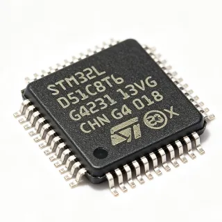
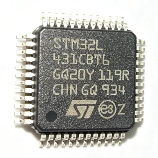
STM32G473CBT6 - 170MHz ARM Cortex-M4F MCU with FPU | STMicroelectronics
MPN: STM32G473CBT6 ✓ Active| Qty | Unit Price | Extended |
|---|---|---|
| 1 | $6.42 | $6.42 |
| 10 | $5.78 | $57.80 |
| 100 | $5.14 | $514.00 |
| 500 | $4.62 | $2,310.00 |
| 1,000 | $4.11 | $4,110.00 |
STM32G473CBT6 Overview
What is a microcontroller? A microcontroller (MCU) is a compact integrated circuit designed to govern a specific operation in an embedded system. It contains a processor core, memory (Flash and SRAM), and programmable input/output peripherals on a single chip. Microcontrollers are the brain of countless electronic devices, from automotive engine control units to home appliances and IoT sensors. In the system hierarchy, a microcontroller sits above simple logic ICs but below application processors, offering a balance of performance, power efficiency, and real-time control capabilities.
Key features of the STM32G473CBT6 include a 170 MHz ARM Cortex-M4F core with DSP instructions and FPU, 128 KB Flash, 32 KB SRAM, and a comprehensive set of communication interfaces: 3x I2C, 4x USART, 3x SPI, 2x FDCAN, 1x USB 2.0 FS, and 1x SAI. It also integrates advanced analog peripherals: 5x 12-bit ADCs with hardware oversampling, 4x 12-bit DACs, 6x operational amplifiers, 7x comparators, and a 16-bit timer with multiple PWM channels. The device supports a supply voltage range of 1.71V to 3.6V and operates over a temperature range of -40°C to +85°C.
The STM32G473CBT6 is built on a high-performance architecture with a nested vectored interrupt controller (NVIC), a memory protection unit (MPU), and a single-cycle multiply-and-accumulate (MAC) unit. It includes a true random number generator (TRNG), a cyclic redundancy check (CRC) unit, and a 128-bit unique device identifier. The device also features a flexible power management with multiple low-power modes (Sleep, Stop, Standby) and a battery backup domain for RTC and 32x32-bit backup registers.
Typical applications include field-oriented control (FOC) of brushless DC (BLDC) motors, digital power supplies (buck, boost, flyback), solar inverters, and industrial automation. The high-resolution timers (HRTIM) with 184 ps resolution make it ideal for power conversion topologies requiring precise PWM generation. The multiple ADCs with simultaneous sampling enable accurate current and voltage sensing in motor control loops.
When designing with this device, pay attention to the decoupling of the VDDA and VREF+ pins to achieve the specified ADC accuracy. Use the internal voltage regulator with external capacitors as recommended in the datasheet. For motor control applications, ensure proper grounding and use the dedicated PWM outputs with complementary signals and dead-time insertion.
Drop-in alternatives for STM32G473CBT6 — same package, pin-to-pin compatible. Different-package parts requiring PCB rework are excluded.
Variants in this series
Same-series models that are drop-in compatible with STM32G473CBT6 (same form factor and footprint) — differing in Communication Interfaces, Core, Package, ADC Resolution, DMA Channels.
Quick Comparison Tool — Select alternative parts for side-by-side comparison:
STM32G474CBT6
✅ Drop-In ⚠️ Specs Unverified📋 Reference alternative (not in catalog)
STM32G431CBT6
✅ Drop-In ⚠️ Specs Unverified✓ In Stock
$3.9773 / Unit
View Datasheet →STM32G441CBT6
✅ Drop-In ⚠️ Specs Unverified✓ In Stock
$2.76 / Unit
View Datasheet →STM32G473CBT6TR
✅ Drop-In ⚠️ Specs Unverified📋 Reference alternative (not in catalog)
STM32G473CBT6 Maximum Ratings & Electrical Characteristics
| Core | ARM Cortex-M4F with FPU |
| Maximum Clock Frequency | 170 MHz |
| Flash Memory | 128 KB |
| SRAM | 32 KB |
| Supply Voltage Range | 1.71 V to 3.6 V |
| Operating Temperature Range | -40C to +85C |
| Package | LQFP-48 (7x7 mm) |
| Number of I/Os | 36 |
| ADC | 5x 12-bit, up to 4 Msps |
| DAC | 4x 12-bit |
| Operational Amplifiers | 6x |
| Comparators | 7x |
| Timers | 1x HRTIM, 4x 16-bit, 2x 32-bit |
| Communication Interfaces | 3x I2C, 4x USART, 3x SPI, 2x FDCAN, 1x USB 2.0 FS, 1x SAI |
| DMA | 2x DMA with 16 channels each |
| RoHS Status | Compliant |
STM32G473CBT6 Pin Configuration
| Pin 1 | VBAT — Battery backup supply for RTC and backup registers |
| Pin 2 | PC13 — GPIO, TAMPER, RTC output |
| Pin 3 | PC14 — GPIO, OSC32_IN |
| Pin 4 | PC15 — GPIO, OSC32_OUT |
| Pin 5 | PF0 — GPIO, OSC_IN |
| Pin 6 | PF1 — GPIO, OSC_OUT |
| Pin 7 | NRST — Reset (active low) |
| Pin 8 | VDDA — Analog power supply |
| Pin 9 | VREF+ — ADC reference voltage |
| Pin 10 | VSSA — Analog ground |
| Pin 11 | PA0 — GPIO, ADC, DAC, TIM2_CH1 |
| Pin 12 | PA1 — GPIO, ADC, DAC, TIM2_CH2 |
| Pin 13 | PA2 — GPIO, ADC, USART2_TX, TIM2_CH3 |
| Pin 14 | PA3 — GPIO, ADC, USART2_RX, TIM2_CH4 |
| Pin 15 | PA4 — GPIO, ADC, DAC, SPI1_NSS |
| Pin 16 | PA5 — GPIO, ADC, DAC, SPI1_SCK |
| Pin 17 | PA6 — GPIO, ADC, SPI1_MISO, TIM3_CH1 |
| Pin 18 | PA7 — GPIO, ADC, SPI1_MOSI, TIM3_CH2 |
| Pin 19 | PB0 — GPIO, ADC, TIM3_CH3 |
| Pin 20 | PB1 — GPIO, ADC, TIM3_CH4 |
| Pin 21 | PB2 — GPIO, BOOT1 |
| Pin 22 | PB10 — GPIO, I2C2_SCL, USART3_TX |
| Pin 23 | PB11 — GPIO, I2C2_SDA, USART3_RX |
| Pin 24 | VSS — Ground |
| Pin 25 | VDD — Power supply |
| Pin 26 | PB12 — GPIO, SPI2_NSS, FDCAN1_RX |
| Pin 27 | PB13 — GPIO, SPI2_SCK, FDCAN1_TX |
| Pin 28 | PB14 — GPIO, SPI2_MISO, TIM12_CH1 |
| Pin 29 | PB15 — GPIO, SPI2_MOSI, TIM12_CH2 |
| Pin 30 | PA8 — GPIO, TIM1_CH1, FDCAN1_RX |
| Pin 31 | PA9 — GPIO, USART1_TX, TIM1_CH2 |
| Pin 32 | PA10 — GPIO, USART1_RX, TIM1_CH3 |
| Pin 33 | PA11 — GPIO, USART1_CTS, USB_DM, TIM1_CH4 |
| Pin 34 | PA12 — GPIO, USART1_RTS, USB_DP, TIM1_ETR |
| Pin 35 | PA13 — GPIO, SWDIO |
| Pin 36 | PA14 — GPIO, SWCLK |
| Pin 37 | PA15 — GPIO, JTDI, TIM2_CH1 |
| Pin 38 | PB3 — GPIO, JTDO, SPI1_SCK |
| Pin 39 | PB4 — GPIO, NJTRST, SPI1_MISO |
| Pin 40 | PB5 — GPIO, SPI1_MOSI, I2C1_SMBA |
| Pin 41 | PB6 — GPIO, I2C1_SCL, USART1_TX |
| Pin 42 | PB7 — GPIO, I2C1_SDA, USART1_RX |
| Pin 43 | BOOT0 — Boot mode selection |
| Pin 44 | PB8 — GPIO, I2C1_SCL, FDCAN1_RX |
| Pin 45 | PB9 — GPIO, I2C1_SDA, FDCAN1_TX |
| Pin 46 | VDD — Power supply |
| Pin 47 | VSS — Ground |
| Pin 48 | VDDA — Analog power supply |
Typical Applications
STM32G473CBT6 is suitable for 6 applications: Field-Oriented Control (FOC) of BLDC Motors, Digital Power Supplies (Buck/Boost Converters), Solar Inverters, Industrial Automation and PLCs, Battery Management Systems (BMS), Test and Measurement Equipment.
Field-Oriented Control (FOC) of BLDC Motors
The STM32G473CBT6 is ideal for FOC of brushless DC motors. Its high-resolution timer (HRTIM) with 184 ps resolution generates precise PWM signals, while the multiple 12-bit ADCs with simultaneous sampling enable accurate current and voltage sensing. The 6 operational amplifiers condition the phase current signals, and the 170 MHz Cortex-M4F core executes the FOC algorithm in real time. The device's 128 KB Flash and 32 KB SRAM provide ample space for control code and data buffers. In a typical FOC application, the MCU reads phase currents via the ADCs, processes them through Clarke and Park transforms, and outputs PWM signals to the inverter. The HRTIM's dead-time insertion prevents shoot-through, and the built-in comparators provide overcurrent protection. The result is smooth, efficient motor control with minimal torque ripple.
Recommended
Digital Power Supplies (Buck/Boost Converters)
The STM32G473CBT6 excels in digital power conversion. Its HRTIM provides high-resolution PWM with 184 ps resolution, essential for precise voltage regulation. The multiple 12-bit ADCs with hardware oversampling enable accurate output voltage and current monitoring. The device's 170 MHz core runs the control loop at high speed, ensuring fast transient response. In a typical buck converter application, the MCU senses the output voltage, compares it to a reference, and adjusts the PWM duty cycle accordingly. The built-in comparators can implement peak current mode control, and the DACs can generate reference voltages. The STM32G473CBT6's rich analog front-end reduces external component count, making the power supply compact and cost-effective. Its wide supply voltage range (1.71V to 3.6V) allows operation from various input rails.
Recommended
Solar Inverters
The STM32G473CBT6 is well-suited for solar inverter applications. Its high-resolution timers and multiple ADCs enable maximum power point tracking (MPPT) and grid synchronization. The device's 170 MHz core can handle complex algorithms like perturb-and-observe MPPT and phase-locked loops. The multiple communication interfaces (FDCAN, USART, SPI) allow connection to monitoring systems and grid communication. The 6 operational amplifiers can condition current and voltage signals from the solar panels and grid. The STM32G473CBT6's robust analog front-end and high-speed PWM generation make it a reliable choice for both string and micro inverters. Its wide operating temperature range (-40°C to +85°C) ensures operation in harsh outdoor environments.
Recommended
Industrial Automation and PLCs
The STM32G473CBT6 is a powerful MCU for industrial automation. Its multiple communication interfaces (FDCAN, USART, SPI, I2C) enable connection to fieldbuses, sensors, and actuators. The 170 MHz Cortex-M4F core with FPU accelerates control algorithms and data processing. The device's rich analog peripherals (ADCs, DACs, op-amps, comparators) allow direct interfacing with analog sensors and actuators. In a PLC, the STM32G473CBT6 can handle multiple I/O points, execute ladder logic, and communicate with a supervisory system via FDCAN. Its robust design, including a true random number generator and CRC unit, ensures reliable operation in industrial environments. The LQFP-48 package is compact, making it suitable for space-constrained PLC modules.
Recommended
Battery Management Systems (BMS)
The STM32G473CBT6 is suitable for battery management systems in electric vehicles and energy storage. Its multiple ADCs can monitor cell voltages and temperatures, while the DACs can generate reference voltages for comparators. The 170 MHz core can execute state-of-charge (SOC) and state-of-health (SOH) algorithms. The FDCAN interface allows communication with the vehicle's main controller. The device's low-power modes (Sleep, Stop, Standby) help conserve battery energy when the system is idle. The STM32G473CBT6's wide supply voltage range (1.71V to 3.6V) allows direct operation from a battery pack. Its robust analog front-end and communication capabilities make it a reliable choice for BMS applications.
Recommended
Test and Measurement Equipment
The STM32G473CBT6 is ideal for test and measurement equipment such as data loggers, signal generators, and oscilloscopes. Its high-speed ADCs (up to 4 Msps) and DACs enable precise signal acquisition and generation. The 170 MHz core with FPU can perform real-time signal processing, such as filtering and FFT. The multiple timers can generate precise trigger signals. The device's USB 2.0 FS interface allows easy connection to a PC for data transfer and control. The STM32G473CBT6's rich peripheral set and high performance make it a versatile choice for portable and benchtop instruments. Its compact LQFP-48 package is suitable for handheld devices.
Recommended
Recommended Products Summary
Engineering reference data for STM32G473CBT6 — comparison, design guidance, and compliance information.
Selection Guide
Comparison with Alternatives
| Parameter | This Product | STM32G474CBT6 | STM32G431CBT6 | STM32G441CBT6 |
|---|---|---|---|---|
| Package | LQFP-48 | LQFP-48 | LQFP-48 | LQFP-48 |
| Brand | STMicroelectronics | STMicroelectronics | STMicroelectronics | STMicroelectronics |
| Core | ARM Cortex-M4F | ARM Cortex-M4F | ARM Cortex-M4F | ARM Cortex-M4F |
| Max Clock Frequency | 170 MHz | 170 MHz | 170 MHz | 170 MHz |
| Flash Memory | 128 KB | 128 KB | 128 KB | 128 KB |
| SRAM | 32 KB | 32 KB | 32 KB | 32 KB |
| Number of ADC Channels | 36 | 42 | 24 | 24 |
| Number of DAC Channels | 4 | 4 | 3 | 3 |
| Number of Op-Amps | 6 | 6 | 4 | 4 |
| Number of Comparators | 7 | 7 | 5 | 5 |
| High-Resolution Timer | Yes (184 ps) | Yes (184 ps) | Yes (184 ps) | Yes (184 ps) |
| USB 2.0 FS | Yes | Yes | No | Yes |
Key Differentiators
- High-resolution timer with 184 ps resolution (vs STM32G431CBT6)
- More ADC channels (36 vs 24) (vs STM32G431CBT6)
- USB 2.0 FS interface (vs STM32G431CBT6)
Design Notes
Decouple the VDDA and VREF+ pins with 1uF and 100nF capacitors placed as close to the pins as possible. Use a ferrite bead between VDD and VDDA to filter high-frequency noise. The internal voltage regulator requires a 1uF capacitor on the VCAP pin (if present) to ensure stable operation. Refer to the STM32G473CB datasheet section on power supply decoupling for recommended values.
For motor control applications, place the power stage (gate drivers, MOSFETs) away from the MCU to minimize noise coupling. Use a star-ground topology for the analog and digital grounds. Route the high-current PWM traces with adequate width and keep them short. Add a ground plane under the MCU to reduce EMI. The LQFP-48 package has a 0.5mm pitch, so use fine-pitch soldering techniques.
Ensure the BOOT0 pin is properly configured to select the correct boot mode. For debugging, connect SWDIO (PA13) and SWCLK (PA14) to the debugger. Do not leave the NRST pin floating; connect a 100nF capacitor to ground. When using the HRTIM, configure the dead-time insertion correctly to prevent shoot-through in the inverter. Also, verify that the ADC sampling time is sufficient for the source impedance of the sensors.
Compliance Information
RoHS compliant per STMicroelectronics product page. Not AEC-Q100 qualified; for automotive, consider STM32G474CBT6 with AEC-Q100 option.