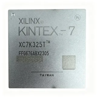
XC7K160T-2FFG676I - Kintex-7 FPGA 162K Logic Cells | AMD
MPN: XC7K160T-2FFG676I ✓ Active| Qty | Unit Price | Extended |
|---|---|---|
| 1 | $108.9 | $108.90 |
| 10 | $98.5 | $985.00 |
| 100 | $89.2 | $8,920.00 |
| 500 | $82.4 | $41,200.00 |
| 1,000 | $76.8 | $76,800.00 |
XC7K160T-2FFG676I Overview
A Field Programmable Gate Array (FPGA) is an integrated circuit that can be configured by the designer after manufacturing, enabling custom digital logic implementations without the cost and lead time of ASIC development. FPGAs sit within the broader hierarchy of programmable logic devices (PLDs), which range from simple CPLDs to high-capacity FPGAs, and are essential in applications requiring parallel processing, rapid prototyping, and field-updatable hardware.
Key features of the XC7K160T-2FFG676I include the -2 speed grade, which balances performance and power consumption, and the FFG676 package that supports easy migration between Kintex-7 family members. The device provides 400 user I/Os, 10 clock management tiles (CMTs) with MMCM and PLL, and 600 DSP slices for high-throughput signal processing. Its 36 Kb block RAM blocks total 11,980,800 bits, enabling substantial on-chip data storage.
Architecturally, the Kintex-7 series is built on a 28 nm high-k metal gate (HKMG) process, offering a strong balance of performance, power, and cost. The -2 speed grade provides a middle ground between the higher-performance -3 and the lower-power -1L/-2L variants. The device supports a wide range of I/O standards, including LVCMOS, LVDS, and HSTL, and includes integrated PCIe, Gigabit transceivers, and DDR3/DDR4 memory interfaces.
Typical applications include high-performance signal processing, software-defined radio, medical imaging, aerospace and defense systems, and wired communications. The 400 I/Os and 162K logic cells make it suitable for complex digital designs requiring substantial parallel processing and connectivity.
When designing with this FPGA, careful attention must be paid to power supply decoupling and thermal management. The FCBGA package requires a well-designed PCB with adequate thermal vias and a solid ground plane to ensure reliable operation at industrial temperatures.
Drop-in alternatives for XC7K160T-2FFG676I — same package, pin-to-pin compatible. Different-package parts requiring PCB rework are excluded.
Variants in this series
Same-series models that are drop-in compatible with XC7K160T-2FFG676I (same form factor and footprint) — differing in Operating Temperature, RoHS Status.
Quick Comparison Tool — Select alternative parts for side-by-side comparison:
XC7K160T-2FF676I
✅ Drop-In📋 Reference alternative (not in catalog)
XC7K160T-1FF676I
✅ Drop-In📋 Reference alternative (not in catalog)
XC7K160T-L2FFG676I
✅ Drop-In📋 Reference alternative (not in catalog)
XC7K325T-2FFG676I
✅ Drop-In✓ In Stock
$98 / Unit
View Datasheet →XC7K160T-2FB676I
✅ Drop-In📋 Reference alternative (not in catalog)
XC7K160T-2FFG676I Maximum Ratings & Electrical Characteristics
| Family | Kintex-7 |
| Logic Cells | 162240 |
| Block RAM | 11980800 bits |
| DSP Slices | 600 |
| User I/Os | 400 |
| Package | 676-BBGA, FCBGA |
| Speed Grade | -2 |
| Operating Temperature | -40°C to +100°C |
| RoHS Status | Lead free / RoHS Compliant |
| Mounting Type | Surface Mount |
| Clock Management Tiles | 10 |
| I/O Standards Supported | LVCMOS, LVDS, HSTL |
XC7K160T-2FFG676I Pin Configuration
| Pin A1 | IO_L1P_T0 — User I/O bank 0 |
| Pin A2 | IO_L1N_T0 — User I/O bank 0 |
| Pin B1 | VCCINT — Internal core voltage |
| Pin B2 | GND — Ground |
| Pin C1 | IO_L2P_T0 — User I/O bank 0 |
| Pin C2 | IO_L2N_T0 — User I/O bank 0 |
| Pin D1 | VCCAUX — Auxiliary voltage |
| Pin D2 | GND — Ground |
| Pin E1 | IO_L3P_T0 — User I/O bank 0 |
| Pin E2 | IO_L3N_T0 — User I/O bank 0 |
| Pin F1 | VCCINT — Internal core voltage |
| Pin F2 | GND — Ground |
Typical Applications
XC7K160T-2FFG676I is suitable for 6 applications: Software Defined Radio, Medical Imaging, Aerospace and Defense, Wired Communications, High-Performance Computing, Industrial Automation.
Software Defined Radio
The XC7K160T-2FFG676I is ideal for software-defined radio (SDR) systems due to its 600 DSP slices and 162,240 logic cells, enabling complex modulation and demodulation algorithms. Its 400 I/Os support multiple ADC/DAC interfaces, while the -2 speed grade ensures real-time processing. The FPGA's parallel architecture allows simultaneous processing of multiple channels, making it suitable for wideband SDR applications. Designers can implement digital down-conversion, filtering, and FFT operations efficiently, leveraging the block RAM for data buffering. The industrial temperature range ensures reliable operation in field-deployed communication equipment.
Recommended
Medical Imaging
In medical imaging systems, the XC7K160T-2FFG676I provides the computational power needed for real-time image processing, such as CT and MRI signal reconstruction. Its 600 DSP slices accelerate filtering and back-projection algorithms, while 11,980,800 bits of block RAM store intermediate image data. The 400 I/Os interface with high-speed ADCs and display controllers, and the -2 speed grade ensures low-latency processing. The FPGA's reconfigurability allows algorithm updates without hardware changes, supporting evolving imaging techniques. The industrial temperature range is suitable for clinical environments.
Recommended
Aerospace and Defense
The XC7K160T-2FFG676I is well-suited for aerospace and defense applications, including radar and electronic warfare systems, due to its high logic density and 400 I/Os. The -2 speed grade supports high-speed signal processing, while the industrial temperature range (-40°C to +100°C) ensures operation in harsh environments. The FPGA's reconfigurability allows in-field updates for changing mission requirements. Its 600 DSP slices handle complex beamforming and pulse compression algorithms, and the block RAM provides on-chip storage for radar data. The lead-free, RoHS-compliant package meets environmental standards for defense electronics.
Recommended
Wired Communications
For wired communications infrastructure, the XC7K160T-2FFG676I offers the logic capacity and I/O count to implement high-speed packet processing and switching. Its 400 I/Os interface with Ethernet PHYs and network processors, while the 600 DSP slices handle traffic shaping and QoS algorithms. The -2 speed grade ensures line-rate processing, and the block RAM supports packet buffering. The FPGA's flexibility allows protocol updates without hardware redesign, making it ideal for evolving standards. The industrial temperature range supports deployment in central offices and data centers.
Recommended
High-Performance Computing
The XC7K160T-2FFG676I is used in high-performance computing (HPC) accelerators, where its 600 DSP slices and 162,240 logic cells accelerate compute-intensive tasks like cryptography and data analytics. The 400 I/Os connect to host processors via PCIe or other high-speed interfaces, and the -2 speed grade provides low-latency processing. The FPGA's parallel architecture enables efficient implementation of custom algorithms, offloading work from CPUs. The block RAM reduces external memory access, improving performance. The industrial temperature range ensures reliability in data center environments.
Recommended
Industrial Automation
In industrial automation, the XC7K160T-2FFG676I provides the logic capacity for implementing motor control, robotics, and machine vision algorithms. Its 400 I/Os interface with sensors, actuators, and cameras, while the 600 DSP slices handle real-time control loops and image processing. The -2 speed grade ensures deterministic response times, and the industrial temperature range supports factory floor environments. The FPGA's reconfigurability allows updates for new automation protocols, and the block RAM stores configuration data. The lead-free, RoHS-compliant package meets environmental regulations.
Recommended
Recommended Products Summary
Engineering reference data for XC7K160T-2FFG676I — comparison, design guidance, and compliance information.
Selection Guide
Comparison with Alternatives
| Parameter | This Product | XC7K160T-2FF676I | XC7K160T-1FF676I | XC7K160T-L2FFG676I | XC7K325T-2FFG676I |
|---|---|---|---|---|---|
| Package | 676-BBGA, FCBGA | 676-BBGA, FCBGA | 676-BBGA, FCBGA | 676-BBGA, FCBGA | 676-BBGA, FCBGA |
| Brand | AMD | AMD | AMD | AMD | AMD |
| Logic Cells | 162240 | 162240 | 162240 | 162240 | 326080 |
| Block RAM (bits) | 11980800 | 11980800 | 11980800 | 11980800 | 16020000 |
| DSP Slices | 600 | 600 | 600 | 600 | 840 |
| User I/Os | 400 | 400 | 400 | 400 | 400 |
| Speed Grade | -2 | -2 | -1 | -2L | -2 |
| Operating Temperature | -40°C to +100°C | -40°C to +100°C | -40°C to +100°C | -40°C to +100°C | -40°C to +100°C |
Key Differentiators
- Lead-free (Green) package (vs XC7K160T-2FF676I)
- Higher speed grade (vs XC7K160T-1FF676I)
- Balanced performance and power (vs XC7K160T-L2FFG676I)
Design Notes
The XC7K160T-2FFG676I requires multiple power rails: VCCINT (core), VCCAUX (auxiliary), and VCCO (I/O banks). Use low-impedance power distribution networks with adequate decoupling capacitors (e.g., 100nF and 10uF) placed close to the FPGA pins. Refer to the Kintex-7 power management application note for recommended capacitor values and placement.
The FCBGA package has a thermal resistance that requires careful thermal management. Ensure a solid thermal path from the package to the PCB using thermal vias and a ground plane. For high-power designs, consider adding a heatsink or active cooling. The industrial temperature range (-40°C to +100°C) must be maintained to ensure reliable operation.
For the 676-ball FCBGA package, use a multi-layer PCB with at least 8 layers to route the 400 I/Os and power planes. Follow AMD's PCB design guidelines for BGA packages, including via-in-pad for high-density routing and proper solder mask openings. Ensure impedance-controlled traces for high-speed signals.
Compliance Information
Lead free / RoHS Compliant per datasheet.