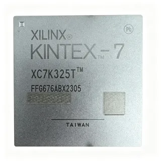
XC7K70T-2FBG676I - Kintex-7 FPGA 65600 Cells | AMD
MPN: XC7K70T-2FBG676I ✓ Active| Qty | Unit Price | Extended |
|---|---|---|
| 1 | $28.87 | $28.87 |
| 10 | $26.5 | $265.00 |
| 100 | $24 | $2,400.00 |
| 500 | $21.5 | $10,750.00 |
| 1,000 | $19 | $19,000.00 |
XC7K70T-2FBG676I Overview
What is an FPGA? An FPGA (Field Programmable Gate Array) is an integrated circuit that can be configured by the customer or designer after manufacturing. Unlike fixed-function ASICs, FPGAs contain an array of programmable logic blocks and interconnects that can be programmed to implement any digital logic function. FPGAs are part of the broader category of programmable logic devices (PLDs), which also includes CPLDs. They are essential in applications requiring rapid prototyping, hardware acceleration, and flexible digital design.
Key features of the XC7K70T-2FBG676I include 300 I/O pins, 5 clock management tiles (CMTs) with MMCM and PLL, and support for various I/O standards. The device also includes 240 DSP48E1 slices for high-speed digital signal processing. The lidless FCBGA package allows for improved thermal performance, making it suitable for high-density designs.
Technically, the Kintex-7 family is optimized for cost-sensitive applications that require high performance. The 28nm process technology enables a balance of speed and power efficiency. The device supports configuration through JTAG, SelectMAP, and SPI interfaces, and is compatible with AMD's Vivado Design Suite for development.
Typical applications include software-defined radio, medical imaging, aerospace and defense systems, and high-performance computing. The XC7K70T is particularly suited for designs that need moderate logic density with high I/O count and DSP capabilities.
When designing with this FPGA, consider power supply decoupling and thermal management. The lidless package requires careful heatsink attachment. Use the provided pinout files from AMD for accurate PCB layout.
Drop-in alternatives for XC7K70T-2FBG676I — same package, pin-to-pin compatible. Different-package parts requiring PCB rework are excluded.
Quick Comparison Tool — Select alternative parts for side-by-side comparison:
XC7K70T-1FBG676I
✅ Drop-In ⚠️ Specs Unverified📋 Reference alternative (not in catalog)
XC7K70T-3FBG676I
✅ Drop-In ⚠️ Specs Unverified📋 Reference alternative (not in catalog)
XC7K70T-2FBG676C
✅ Drop-In ⚠️ Specs Unverified📋 Reference alternative (not in catalog)
XC7K70T-2FBG676E
✅ Drop-In ⚠️ Specs Unverified📋 Reference alternative (not in catalog)
XC7K70T-2FBG676I
✅ Drop-In✓ In Stock
$19 / Unit
View Datasheet →XC7K70T-2FBG676I Maximum Ratings & Electrical Characteristics
| Family | Kintex-7 |
| Logic Cells | 65600 |
| Number of I/Os | 300 |
| Block RAM | 4976640 bits |
| DSP Slices | 240 |
| CMTs | 5 |
| Technology | 28nm |
| Core Voltage | 1V |
| Package | 676-BBGA, FCBGA |
| Mounting Type | Surface Mount |
| Operating Temperature | -40C to +100C |
| RoHS Status | Compliant |
| Speed Grade | -2 |
| Configuration Interfaces | JTAG, SelectMAP, SPI |
| I/O Standards | LVCMOS, LVDS, HSTL, SSTL |
XC7K70T-2FBG676I Pin Configuration
| Pin A1 | IO_L1P_T0 — User I/O bank 0 |
| Pin A2 | IO_L1N_T0 — User I/O bank 0 |
| Pin B1 | IO_L2P_T0 — User I/O bank 0 |
| Pin B2 | IO_L2N_T0 — User I/O bank 0 |
| Pin C1 | IO_L3P_T0 — User I/O bank 0 |
| Pin C2 | IO_L3N_T0 — User I/O bank 0 |
| Pin D1 | IO_L4P_T0 — User I/O bank 0 |
| Pin D2 | IO_L4N_T0 — User I/O bank 0 |
| Pin E1 | IO_L5P_T0 — User I/O bank 0 |
| Pin E2 | IO_L5N_T0 — User I/O bank 0 |
| Pin F1 | IO_L6P_T0 — User I/O bank 0 |
| Pin F2 | IO_L6N_T0 — User I/O bank 0 |
Typical Applications
XC7K70T-2FBG676I is suitable for 6 applications: Software-Defined Radio, Medical Imaging, Aerospace and Defense, High-Performance Computing, Wired Communications, Test and Measurement.
Software-Defined Radio
The XC7K70T-2FBG676I is ideal for software-defined radio (SDR) systems due to its 240 DSP48E1 slices and high-speed transceivers. It can handle complex modulation schemes and digital down/up conversion. The 300 I/Os allow interfacing with multiple ADCs and DACs. Its 28nm technology provides low power consumption, essential for portable SDR units. The FPGA's reconfigurability enables over-the-air updates and multi-standard support.
Recommended
Medical Imaging
In medical imaging systems like ultrasound and CT scanners, the XC7K70T-2FBG676I provides the necessary DSP bandwidth for image processing. Its 240 DSP slices accelerate filtering and beamforming algorithms. The 4,976,640 bits of block RAM support frame buffering. The industrial temperature grade ensures reliability in clinical environments. The FPGA's parallel processing capability enables real-time image enhancement.
Recommended
Aerospace and Defense
The XC7K70T-2FBG676I is suitable for aerospace and defense applications such as radar and secure communications. Its 28nm technology offers high performance with low power, critical for airborne systems. The device supports radiation-tolerant configurations with proper mitigation. The 300 I/Os allow interfacing with various sensors and communication links. AMD's long-term supply commitment ensures availability for defense programs.
Recommended
High-Performance Computing
For high-performance computing (HPC) accelerators, the XC7K70T-2FBG676I offers 240 DSP slices and 65,600 logic cells for parallel processing. It can be used for data compression, encryption, and machine learning inference. The 4,976,640 bits of block RAM provide on-chip storage for frequently accessed data. The FPGA's reconfigurability allows algorithm updates without hardware changes. Its 1V core voltage reduces power consumption in data centers.
Recommended
Wired Communications
In wired communication systems like switches and routers, the XC7K70T-2FBG676I provides high-speed serial transceivers and flexible I/O. It can implement packet processing, traffic management, and protocol conversion. The 300 I/Os support various memory interfaces and network PHYs. The FPGA's low latency is essential for real-time packet forwarding. Its 28nm technology balances performance and power for line-card designs.
Recommended
Test and Measurement
The XC7K70T-2FBG676I is used in test and measurement equipment like oscilloscopes and logic analyzers. Its high-speed I/Os and DSP capabilities enable signal acquisition and analysis. The 240 DSP slices accelerate FFT and filtering operations. The FPGA's reconfigurability allows firmware updates to add new measurement features. The industrial temperature grade ensures stable operation in lab environments.
Recommended
Recommended Products Summary
Engineering reference data for XC7K70T-2FBG676I — comparison, design guidance, and compliance information.
Selection Guide
Comparison with Alternatives
| Parameter | This Product | XC7K70T-1FBG676I | XC7K70T-3FBG676I | XC7K70T-2FBG676C |
|---|---|---|---|---|
| Package | 676-BBGA, FCBGA | 676-BBGA, FCBGA | 676-BBGA, FCBGA | 676-BBGA, FCBGA |
| Brand | AMD | AMD | AMD | AMD |
| Speed Grade | -2 | -1 | -3 | -2 |
| Temperature Grade | Industrial (-40C to +100C) | Industrial | Industrial | Commercial (0C to +85C) |
| Logic Cells | 65600 | 65600 | 65600 | 65600 |
| Block RAM | 4976640 bits | 4976640 bits | 4976640 bits | 4976640 bits |
| DSP Slices | 240 | 240 | 240 | 240 |
| I/O Count | 300 | 300 | 300 | 300 |
Key Differentiators
- Higher speed grade than -1 (vs XC7K70T-1FBG676I)
- Industrial temperature grade (vs XC7K70T-2FBG676C)
- Balanced performance and cost (vs XC7K70T-3FBG676I)
Design Notes
The XC7K70T-2FBG676I requires multiple power rails: VCCINT at 1.0V, VCCAUX at 1.8V, and VCCO depending on I/O banks. Use a dedicated power management IC to sequence these rails. Decouple each rail with 100nF and 10uF capacitors near the FPGA pins. Refer to the 7 Series FPGAs Power Management User Guide (UG473) for detailed recommendations.
The lidless FCBGA package requires a heatsink for high-power designs. The thermal resistance (theta_JA) is approximately 10 C/W without airflow. For a 5W design, the junction temperature rise is 50C above ambient. Ensure adequate airflow or a heatsink to keep junction temperature below 100C. Use thermal interface material between the die and heatsink.
For the 676-pin FCBGA, use a high-layer-count PCB (at least 8 layers) for routing. Follow AMD's PCB design guidelines in UG483. Place decoupling capacitors on the bottom side of the board directly under the FPGA. Use via-in-pad for power and ground connections. Ensure controlled impedance for high-speed signals.
Compliance Information
RoHS compliant per AMD product page. Not AEC-Q100 qualified as it is not an automotive part.