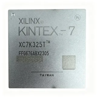
XC7K325T-1FFG676C - Kintex-7 FPGA 326K Cells | AMD
MPN: XC7K325T-1FFG676C ✓ Active| Qty | Unit Price | Extended |
|---|---|---|
| 1 | $495 | $495.00 |
| 10 | $460 | $4,600.00 |
| 100 | $420 | $42,000.00 |
| 500 | $380 | $190,000.00 |
| 1,000 | $350 | $350,000.00 |
XC7K325T-1FFG676C Overview
A Field Programmable Gate Array (FPGA) is an integrated circuit that can be configured by the customer after manufacturing to implement arbitrary digital logic functions. FPGAs sit within the broader hierarchy of programmable logic devices (PLDs), which are a subset of application-specific integrated circuits (ASICs) but offer reconfigurability. The Kintex-7 family is positioned as the best price/performance/watt balance in the 7-series, bridging the gap between the low-cost Artix-7 and the high-end Virtex-7.
Key features include 840 DSP48E1 slices for high-throughput signal processing, 500 MHz maximum clock frequency, and support for DDR3 memory interfaces. The device integrates 10.3 Gbps transceivers (GTX) for high-speed serial communication, and includes hardened blocks for PCIe Gen3 and 10G Ethernet MAC. The -1 speed grade provides a balanced performance point, while the C temperature grade supports commercial operation from 0°C to 85°C.
Architecturally, the Kintex-7 uses a 6-input look-up table (LUT) fabric with 203,800 LUTs, organized into configurable logic blocks (CLBs). The device includes 10 clock management tiles (CMTs) with mixed-mode clock managers (MMCMs) and phase-locked loops (PLLs) for flexible clock generation. The 28nm high-k metal gate (HKMG) process technology delivers up to 50% lower power than previous generations while maintaining high logic density.
Typical applications include software-defined radio, high-performance computing acceleration, video and image processing, and wired communications infrastructure. The 400 I/Os support a wide range of I/O standards including LVCMOS, LVDS, and HSTL, making it versatile for board-level integration.
When designing with this device, careful attention to power supply decoupling is essential. The core voltage must be regulated to 1.0V with adequate bypass capacitance, and the configuration bitstream must be loaded from an external SPI flash or via JTAG. Thermal management is critical at high utilization; a heatsink or forced airflow is recommended for sustained operation above 50% logic utilization.
Drop-in alternatives for XC7K325T-1FFG676C — same package, pin-to-pin compatible. Different-package parts requiring PCB rework are excluded.
Variants in this series
Same-series models that are drop-in compatible with XC7K325T-1FFG676C (same form factor and footprint) — differing in Core Voltage, Operating Temperature, Speed Grade, Mounting Type.
Quick Comparison Tool — Select alternative parts for side-by-side comparison:
XC7K325T-2FFG676C
✅ Drop-In📋 Reference alternative (not in catalog)
XC7K325T-1FFG676I
✅ Drop-In📋 Reference alternative (not in catalog)
XC7K325T-3FFG676E
✅ Drop-In📋 Reference alternative (not in catalog)
XC7K325T-1FBG676C
✅ Drop-In✓ In Stock
$108 / Unit
View Datasheet →CWC2P300T-FFG676I
✅ Drop-In ⚠️ Specs Unverified📋 Reference alternative (not in catalog)
XC7K325T-1FFG676C Maximum Ratings & Electrical Characteristics
| Family | Kintex-7 |
| Logic Cells | 326080 |
| Number of I/Os | 400 |
| Block RAM | 16404480 bits |
| DSP Slices | 840 |
| LUTs | 203800 |
| Maximum Clock Frequency | 400 MHz |
| Core Voltage | 0.97 V to 1.03 V |
| Package | 676-BBGA, FCBGA |
| Operating Temperature | 0°C to 85°C |
| Process Technology | 28nm |
| Speed Grade | -1 |
| Transceivers | 16 GTX (10.3 Gbps) |
| PCIe Support | Gen3 |
| Configuration | SRAM-based, external flash |
| RoHS Status | Compliant |
XC7K325T-1FFG676C Pin Configuration
| Pin A1 | IO_L1P_T0 — User I/O differential pair P |
| Pin A2 | IO_L1N_T0 — User I/O differential pair N |
| Pin B1 | VCCINT — Internal core voltage 1.0V |
| Pin B2 | GND — Ground |
| Pin C1 | IO_L2P_T1 — User I/O differential pair P |
| Pin C2 | IO_L2N_T1 — User I/O differential pair N |
| Pin D1 | VCCAUX — Auxiliary voltage 1.8V |
| Pin D2 | GND — Ground |
| Pin E1 | IO_L3P_T2 — User I/O differential pair P |
| Pin E2 | IO_L3N_T2 — User I/O differential pair N |
| Pin F1 | VCCBRAM — Block RAM voltage 1.0V |
| Pin F2 | GND — Ground |
Typical Applications
XC7K325T-1FFG676C is suitable for 6 applications: Software-Defined Radio, High-Performance Computing Acceleration, Video and Image Processing, Wired Communications Infrastructure, Test and Measurement Equipment, Aerospace and Defense.
Software-Defined Radio
The XC7K325T-1FFG676C excels in SDR platforms due to its 840 DSP slices and 16 GTX transceivers. The DSP slices handle digital down-conversion, filtering, and modulation, while the transceivers interface with high-speed ADCs/DACs at up to 10.3 Gbps. The 400 I/Os connect to multiple RF front-ends, and the 16.4 Mb block RAM supports large FFT buffers. This combination enables wideband signal processing for military and commercial communications, with the -1 speed grade providing adequate performance while minimizing power in field-deployed systems.
Recommended
High-Performance Computing Acceleration
In HPC acceleration, the XC7K325T-1FFG676C provides 326K logic cells and 840 DSP slices for custom arithmetic pipelines. Its 16 GTX transceivers enable high-bandwidth data movement between FPGAs or to host processors via PCIe Gen3. The 400 I/Os support wide parallel interfaces to HBM or SRAM. The 28nm process delivers a balance of density and power, making it suitable for rack-mounted accelerators where thermal budgets are tight. The -1 speed grade is often sufficient for integer and fixed-point workloads, reducing cost compared to -2 or -3 grades.
Recommended
Video and Image Processing
The XC7K325T-1FFG676C is ideal for video processing pipelines, offering 400 I/Os to connect multiple camera sensors or display interfaces. The 840 DSP slices perform real-time filtering, scaling, and color space conversion, while the 16.4 Mb block RAM provides line buffers and frame storage. The GTX transceivers support SDI or 10G Ethernet for video transport. The 28nm process enables high logic density for complex algorithms like H.264 encoding or computer vision, and the -1 speed grade is adequate for 1080p60 or 4K30 processing, balancing performance and power.
Recommended
Wired Communications Infrastructure
For wired communications, the XC7K325T-1FFG676C supports PCIe Gen3 and 10G Ethernet natively, making it a strong choice for network interface cards, switches, and routers. The 16 GTX transceivers handle multiple 10G links, while the 400 I/Os connect to PHYs and management interfaces. The 326K logic cells accommodate packet processing, forwarding, and traffic management. The 28nm process provides the performance needed for line-rate processing at 10G, and the -1 speed grade is often sufficient for non-blocking switching fabrics, offering cost savings over higher speed grades.
Recommended
Test and Measurement Equipment
The XC7K325T-1FFG676C is well-suited for test and measurement instruments like oscilloscopes, logic analyzers, and signal generators. Its 400 I/Os connect to high-speed ADCs and DACs, while the 840 DSP slices perform real-time signal analysis, triggering, and waveform generation. The 16.4 Mb block RAM supports deep acquisition buffers. The GTX transceivers enable high-speed data streaming to a host PC. The -1 speed grade provides sufficient performance for most benchtop instruments, and the commercial temperature range is adequate for lab environments, keeping cost down.
Recommended
Aerospace and Defense
In aerospace and defense, the XC7K325T-1FFG676C is used for radar, electronic warfare, and secure communications. The 840 DSP slices handle pulse compression and beamforming, while the 16 GTX transceivers support high-speed sensor interfaces. The 400 I/Os connect to various avionics buses. The 28nm process offers a good balance of performance and power for airborne platforms. While the commercial temperature grade (C) is limited to 0-85°C, the pin-compatible industrial (I) version is available for extended environments. The -1 speed grade is often chosen for its lower power consumption in battery or generator-limited systems.
Recommended
Recommended Products Summary
Engineering reference data for XC7K325T-1FFG676C — comparison, design guidance, and compliance information.
Selection Guide
Comparison with Alternatives
| Parameter | This Product | XC7K325T-2FFG676C | XC7K325T-1FFG676I | XC7K325T-3FFG676E | XC7K325T-1FBG676C | CWC2P300T-FFG676I |
|---|---|---|---|---|---|---|
| Package | 676-BBGA, FCBGA | 676-BBGA, FCBGA - same | 676-BBGA, FCBGA - same | 676-BBGA, FCBGA - same | 676-BBGA, FCBGA - same | 676-BBGA, FCBGA - same |
| Brand | AMD | AMD | AMD | AMD | AMD | Chengdu Sinochip |
| Logic Cells | 326080 | 326080 | 326080 | 326080 | 326080 | 300000 |
| Speed Grade | -1 | -2 | -1 | -3 | -1 | -1 |
| Temperature Range | 0°C to 85°C | 0°C to 85°C | -40°C to 100°C | -40°C to 125°C | 0°C to 85°C | -40°C to 100°C |
Key Differentiators
- Balanced price/performance/watt at 28nm (vs XC7K325T-2FFG676C)
- Commercial temperature grade for cost savings (vs XC7K325T-1FFG676I)
- Native PCIe Gen3 and 10G Ethernet support (vs CWC2P300T-FFG676I)
Design Notes
The XC7K325T-1FFG676C requires a 1.0V core supply (VCCINT) with tight regulation (0.97V to 1.03V). Use a dedicated switching regulator with at least 10A capability and place 100nF and 10uF ceramic capacitors close to each VCCINT pin. The VCCAUX rail (1.8V) and VCCBRAM (1.0V) also need proper decoupling. Refer to AMD's UG583 for detailed power supply design guidelines.
At 50% logic utilization and 400 MHz, the XC7K325T-1FFG676C can dissipate 5-10W. The FCBGA package has a thermal resistance of approximately 8-10°C/W (theta_JA) without airflow. For sustained operation, attach a heatsink or provide forced airflow to keep junction temperature below 85°C. Use AMD's Power Estimator to calculate exact dissipation for your design.
The 676-pin FCBGA requires a multi-layer PCB with at least 8 layers for proper routing and power integrity. Use 0.8mm via diameter and 0.4mm drill for signal vias. Route high-speed transceiver pairs with controlled impedance (100 ohm differential) and keep them away from clock signals. Follow AMD's PCB design guidelines in UG583 for layout best practices.
Compliance Information
RoHS compliant per AMD product page. Not AEC-Q100 qualified (FPGA, not automotive). Lead-free and halogen-free per AMD environmental data.