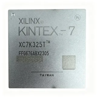
XC7K325T-1FBG676C - Kintex-7 FPGA 326K Logic Cells | AMD
MPN: XC7K325T-1FBG676C ✓ Active| Qty | Unit Price | Extended |
|---|---|---|
| 1 | $157.63 | $157.63 |
| 10 | $145.2 | $1,452.00 |
| 100 | $132.8 | $13,280.00 |
| 500 | $120.4 | $60,200.00 |
| 1,000 | $108 | $108,000.00 |
XC7K325T-1FBG676C Overview
An FPGA (Field Programmable Gate Array) is an integrated circuit that can be configured by the customer after manufacturing to implement any digital logic function. FPGAs sit between ASICs (application-specific) and microprocessors (fixed-function) in the design hierarchy, offering reconfigurability and parallel processing. The Kintex-7 family is optimized for price/performance/watt, balancing logic density, DSP capability, and transceiver performance for mid-range to high-end applications.
Key features include 400 I/O pins, 16,404,480 bits of block RAM, and 326,080 logic cells. The device supports multiple speed grades (-1, -2, -3) and includes hardened blocks for PCIe, Gigabit Ethernet, and DDR3 memory controllers. The 676-ball FCBGA package provides excellent thermal and electrical performance for high-speed designs.
Architecturally, the Kintex-7 uses a 6-input look-up table (LUT) fabric with dedicated carry chains, DSP48E1 slices for multiply-accumulate operations, and configurable block RAM. The device integrates Clock Management Tiles (CMTs) with MMCM and PLL for precise clock generation. The 28nm HPL process enables low static power while maintaining high performance.
Typical applications include software-defined radio, high-performance computing, video processing, and aerospace/defense systems. The device's high DSP ratio and transceiver capabilities make it ideal for signal processing and data acquisition. Its support for PCIe Gen2 and DDR3 simplifies system integration.
When designing with this FPGA, careful attention to power supply decoupling and thermal management is essential. The core voltage must be maintained within 0.97V to 1.03V, and the FCBGA package requires a proper thermal solution for high utilization designs.
Drop-in alternatives for XC7K325T-1FBG676C — same package, pin-to-pin compatible. Different-package parts requiring PCB rework are excluded.
Variants in this series
Same-series models that are drop-in compatible with XC7K325T-1FBG676C (same form factor and footprint) — differing in Core Voltage, Operating Temperature, Speed Grade, Mounting Type.
Quick Comparison Tool — Select alternative parts for side-by-side comparison:
XC7K325T-2FBG676C
✅ Drop-In✓ In Stock
$780 / Unit
View Datasheet →XC7K325T-1FBG676I
✅ Drop-In📋 Reference alternative (not in catalog)
XC7K325T-1FFG676C
✅ Drop-In✓ In Stock
$350 / Unit
View Datasheet →CWC2P300T-FFG676I
✅ Drop-In ⚠️ Specs Unverified📋 Reference alternative (not in catalog)
XC7K325T-1FBG676C Maximum Ratings & Electrical Characteristics
| Family | Kintex-7 |
| Logic Cells | 326080 |
| Block RAM | 16404480 bits |
| Number of I/Os | 400 |
| Package | 676-BBGA, FCBGA |
| Core Voltage | 1.0 V (0.97V to 1.03V) |
| Technology | 28nm |
| Speed Grade | -1 |
| Maximum Frequency | 400 MHz |
| Operating Temperature | 0C to +85C |
| Mounting Type | Surface Mount |
| RoHS Status | Compliant |
| REACH Status | Compliant |
| Series | Kintex-7 |
| Number of Logic Elements | 326080 |
XC7K325T-1FBG676C Pin Configuration
| Pin A1 | IO_L1P_T0 — User I/O bank 0, differential pair P |
| Pin A2 | IO_L1N_T0 — User I/O bank 0, differential pair N |
| Pin B1 | IO_L2P_T0 — User I/O bank 0, differential pair P |
| Pin B2 | IO_L2N_T0 — User I/O bank 0, differential pair N |
| Pin C1 | VCCINT — Internal core voltage 1.0V |
| Pin C2 | GND — Ground |
| Pin D1 | VCCAUX — Auxiliary voltage 1.8V |
| Pin D2 | GND — Ground |
| Pin E1 | IO_L3P_T0 — User I/O bank 0, differential pair P |
| Pin E2 | IO_L3N_T0 — User I/O bank 0, differential pair N |
| Pin F1 | IO_L4P_T0 — User I/O bank 0, differential pair P |
| Pin F2 | IO_L4N_T0 — User I/O bank 0, differential pair N |
Typical Applications
XC7K325T-1FBG676C is suitable for 6 applications: Software Defined Radio, High-Performance Computing, Video Processing, Aerospace and Defense, Data Acquisition and Instrumentation, Telecommunications Infrastructure.
Software Defined Radio
The XC7K325T-1FBG676C excels in software-defined radio (SDR) systems due to its high DSP ratio and 400 I/Os. With 326,080 logic cells and 16.4 Mb of block RAM, it can implement complex digital down-conversion, filtering, and modulation algorithms. The 28nm process enables low power consumption, critical for portable and field-deployed radios. The device supports multiple high-speed serial transceivers for ADC/DAC interfaces, and its MMCM/PLL blocks provide precise clock generation for RF sampling. This FPGA enables reconfigurable waveforms and multi-standard support, making it ideal for military and commercial SDR platforms.
Recommended
High-Performance Computing
In high-performance computing (HPC), the XC7K325T-1FBG676C provides massive parallel processing capabilities with 326,080 logic cells. Its DSP48E1 slices enable efficient multiply-accumulate operations for scientific computing, financial modeling, and data analytics. The 400 I/Os support high-bandwidth memory interfaces like DDR3, and the 28nm technology balances performance with power efficiency. The device can accelerate algorithms by 10-100x compared to CPUs for specific workloads. Its PCIe support enables seamless integration into server systems, making it a cost-effective accelerator for data centers and research institutions.
Recommended
Video Processing
The XC7K325T-1FBG676C is well-suited for video processing applications, offering 400 I/Os and 16.4 Mb of block RAM for frame buffering. Its 326,080 logic cells can implement complex video codecs, image scaling, and real-time enhancement algorithms. The device supports multiple video standards through its flexible I/O, and the 28nm process enables low-latency processing. With support for PCIe and DDR3, it can handle 4K video streams at 60fps. The MMCM/PLL blocks generate precise pixel clocks, ensuring synchronization across multiple video channels. This makes it ideal for broadcast, medical imaging, and surveillance systems.
Recommended
Aerospace and Defense
The XC7K325T-1FBG676C is designed for aerospace and defense applications, offering high reliability and performance in a 676-FCBGA package. Its 326,080 logic cells support complex radar, sonar, and electronic warfare processing. The device operates over the commercial temperature range (0C to +85C) and can be paired with industrial-grade variants for harsher environments. The 28nm technology provides radiation tolerance suitable for many defense applications. With 400 I/Os, it interfaces with a wide range of sensors and communication systems. The FPGA's reconfigurability allows for in-field updates, critical for evolving mission requirements.
Recommended
Data Acquisition and Instrumentation
The XC7K325T-1FBG676C is ideal for data acquisition systems, providing 400 I/Os for interfacing with high-speed ADCs and DACs. Its 326,080 logic cells enable real-time signal processing, triggering, and data reduction. The 16.4 Mb block RAM supports large data buffers, while the 28nm process ensures low power for portable instruments. The device's MMCM/PLL blocks generate precise sampling clocks, critical for accurate measurements. With PCIe support, it can stream data to host computers at high rates. This makes it suitable for oscilloscopes, spectrum analyzers, and scientific instruments.
Recommended
Telecommunications Infrastructure
The XC7K325T-1FBG676C is a key component in telecommunications infrastructure, offering high-speed serial transceivers and 400 I/Os for backplane and line card interfaces. Its 326,080 logic cells implement packet processing, error correction, and protocol conversion. The device supports PCIe and Gigabit Ethernet, enabling seamless integration into network equipment. The 28nm technology provides the performance needed for 100G+ systems while managing power consumption. With 16.4 Mb of block RAM, it can buffer large packets and support Quality of Service (QoS) algorithms. This makes it ideal for routers, switches, and base stations.
Recommended
Recommended Products Summary
Engineering reference data for XC7K325T-1FBG676C — comparison, design guidance, and compliance information.
Selection Guide
Comparison with Alternatives
| Parameter | This Product | XC7K325T-2FBG676C | XC7K325T-1FBG676I | XC7K325T-1FFG676C | CWC2P300T-FFG676I |
|---|---|---|---|---|---|
| Package | 676-FCBGA (FBG) | 676-FCBGA (FBG) | 676-FCBGA (FBG) | 676-FCBGA (FFG) | 676-FCBGA (FFG) |
| Brand | AMD | AMD | AMD | AMD | Chengdu Sino Microelectronics |
Key Differentiators
- Higher speed grade option (vs XC7K325T-1FBG676C vs XC7K325T-2FBG676C)
- Industrial temperature range (vs XC7K325T-1FBG676C vs XC7K325T-1FBG676I)
- Lidless package for thermal performance (vs XC7K325T-1FBG676C vs XC7K325T-1FFG676C)
Design Notes
The XC7K325T-1FBG676C requires a 1.0V core supply (VCCINT) with tight regulation (0.97V to 1.03V). Use a dedicated switching regulator with remote sensing to maintain accuracy under dynamic load. Decouple each VCCINT pin with a 100nF ceramic capacitor and add bulk capacitance (10uF) per power region. The VCCAUX rail (1.8V) should be similarly decoupled. Follow AMD's power distribution network (PDN) guidelines in UG583 for optimal performance.
The 676-FCBGA package has a thermal resistance that requires careful management. For high-utilization designs, use a heatsink with forced airflow. The lidless FBG package allows direct contact with the die for improved thermal performance. Calculate power dissipation using AMD's Power Estimator tool and ensure junction temperature stays below 85C for commercial grade. Consider the thermal vias under the package for heat spreading to the PCB ground plane.
For the 676-FCBGA package, use a high-layer-count PCB (12-16 layers) with controlled impedance for high-speed signals. Route differential pairs with 100-ohm impedance for transceivers. Place decoupling capacitors on the bottom side directly under the BGA pads. Follow AMD's PCB design guidelines in UG583 for stack-up, via placement, and signal integrity. Use the package pinout files from AMD for accurate footprint creation.
Compliance Information
RoHS and REACH compliant per distributor data. Not AEC-Q100 qualified as it is not an automotive-grade part.