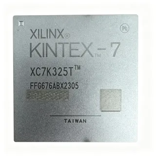
XC7K325T-2FBG676C - Kintex-7 FPGA 326K Logic Cells | AMD
MPN: XC7K325T-2FBG676C ✓ Active| Qty | Unit Price | Extended |
|---|---|---|
| 1 | $1200 | $1,200.00 |
| 10 | $1100 | $11,000.00 |
| 100 | $950 | $95,000.00 |
| 500 | $850 | $425,000.00 |
| 1,000 | $780 | $780,000.00 |
XC7K325T-2FBG676C Overview
An FPGA (Field Programmable Gate Array) is an integrated circuit that can be configured by the customer or designer after manufacturing. Unlike fixed-function ASICs, FPGAs contain an array of programmable logic blocks, configurable I/O, and routing resources that can be programmed to implement any digital logic function. The Kintex-7 family sits in the mid-range of the 7 series, balancing logic capacity, DSP slices, and transceiver performance to address applications from cost-sensitive, high-volume systems to ultra high-end connectivity and signal processing. This places the XC7K325T within the hierarchy of FPGA -> programmable logic device -> integrated circuit -> semiconductor.
Key features of the XC7K325T-2FBG676C include 400 user I/O pins, 25475 Configurable Logic Blocks (CLBs), and 326,080 logic elements/cells. The device also integrates 16,404,480 bits of block RAM, enabling substantial on-chip data storage for buffering and processing. The -2 speed grade offers a balanced performance point, with the -3 grade being the highest performance and -1/-1L for lower power. The 676-FCBGA package provides a compact footprint while supporting the high pin count required for parallel interfaces and memory controllers.
From a technical architecture perspective, the Kintex-7 family is built on a 28nm high-k metal gate (HKMG) process, offering a strong price/performance/watt ratio. The device includes hardened blocks such as DSP48E1 slices for high-speed arithmetic, and supports mainstream standards like PCIe Gen3 and 10 Gigabit Ethernet via its high-speed transceivers. The lidless FCBGA package aids in thermal management, allowing direct heatsink attachment for improved heat dissipation in high-power designs.
Typical applications for the XC7K325T-2FBG676C include software-defined radio, high-performance computing, medical imaging, and aerospace/defense systems. Its combination of logic density, DSP capability, and I/O count makes it suitable for implementing complex digital signal processing chains, protocol bridging, and parallel processing architectures. The device is also commonly used in development boards like the QMTECH XC7K325T for prototyping and algorithm validation.
When designing with this FPGA, careful attention must be paid to power supply decoupling and thermal management. The device requires multiple supply rails (VCCINT, VCCAUX, VCCO) with appropriate filtering, and the lidless package should be paired with a suitable heatsink for applications exceeding moderate power dissipation. Refer to the AMD 7 Series FPGAs datasheet and UG475 for detailed pinout and power requirements.
Drop-in alternatives for XC7K325T-2FBG676C — same package, pin-to-pin compatible. Different-package parts requiring PCB rework are excluded.
Variants in this series
Same-series models that are drop-in compatible with XC7K325T-2FBG676C (same form factor and footprint) — differing in Operating Temperature, Core Voltage, Speed Grade, Mounting Type.
Quick Comparison Tool — Select alternative parts for side-by-side comparison:
XC7K325T-1FBG676C
✅ Drop-In✓ In Stock
$108 / Unit
View Datasheet →XC7K325T-3FBG676C
✅ Drop-In ⚠️ Specs Unverified📋 Reference alternative (not in catalog)
XC7K325T-1FFG676C
✅ Drop-In✓ In Stock
$350 / Unit
View Datasheet →XC7K325T-2FFG676C
✅ Drop-In ⚠️ Specs Unverified📋 Reference alternative (not in catalog)
XC7K325T-2FFG676I
✅ Drop-In ⚠️ Specs Unverified✓ In Stock
$98 / Unit
View Datasheet →XC7K325T-2FBG676C Maximum Ratings & Electrical Characteristics
| Family | Kintex-7 |
| Number of Logic Elements/Cells | 326080 |
| Number of LABs/CLBs | 25475 |
| Total RAM Bits | 16404480 |
| Number of I/O | 400 |
| Package / Case | 676-BBGA, FCBGA |
| Package Size | 27x27 mm |
| Mounting Type | Surface Mount (SMD/SMT) |
| Operating Temperature | 0°C to 85°C (TJ) |
| Speed Grade | -2 |
| Process Technology | 28nm |
| Core Voltage | 1V |
| Status | Active |
| Categories | Integrated Circuits |
XC7K325T-2FBG676C Pin Configuration
| Pin A1 | IO_L1P_T0 — User I/O bank 0, differential pair P |
| Pin A2 | IO_L1N_T0 — User I/O bank 0, differential pair N |
| Pin B1 | VCCINT — Internal core voltage supply |
| Pin B2 | GND — Ground |
| Pin C1 | IO_L2P_T0 — User I/O bank 0, differential pair P |
| Pin C2 | IO_L2N_T0 — User I/O bank 0, differential pair N |
| Pin D1 | VCCO_0 — I/O bank 0 supply voltage |
| Pin D2 | GND — Ground |
| Pin E1 | IO_L3P_T0 — User I/O bank 0, differential pair P |
| Pin E2 | IO_L3N_T0 — User I/O bank 0, differential pair N |
| Pin F1 | VCCAUX — Auxiliary supply voltage |
| Pin F2 | GND — Ground |
Typical Applications
XC7K325T-2FBG676C is suitable for 6 applications: Software-Defined Radio, High-Performance Computing, Medical Imaging, Aerospace and Defense, Wired and Wireless Networking, Test and Measurement.
Software-Defined Radio
The XC7K325T-2FBG676C is ideal for software-defined radio (SDR) systems due to its 326,080 logic cells and 400 I/Os, which enable complex DSP chains, FFTs, and digital up/down converters. The -2 speed grade supports high sample rates, and the 28nm process offers good power efficiency. In an SDR, the FPGA handles baseband processing, channelization, and modulation/demodulation, replacing multiple fixed-function ICs. Its block RAM (16.4 Mb) supports buffering of wideband signals, while the high I/O count interfaces with high-speed ADCs and DACs. The lidless FCBGA package aids thermal management in rack-mounted units, ensuring reliable operation in continuous-duty environments.
Recommended
High-Performance Computing
In high-performance computing (HPC), the XC7K325T-2FBG676C accelerates custom algorithms by providing massive parallelism. With 326,080 logic cells and 400 I/Os, it can implement multiple processing elements, custom arithmetic units, and high-bandwidth interfaces. The -2 speed grade ensures fast clock rates for compute-intensive tasks, while the 28nm process balances performance and power. The FPGA's block RAM supports local data storage, reducing memory latency. It is commonly used in financial modeling, scientific simulations, and data analytics, where reconfigurable hardware can outperform general-purpose CPUs for specific workloads. The 676-FCBGA package allows dense board layouts, and the lidless design facilitates heatsink attachment for sustained high-performance operation.
Recommended
Medical Imaging
The XC7K325T-2FBG676C is well-suited for medical imaging systems like ultrasound and MRI, where real-time signal processing is critical. Its 326,080 logic cells enable implementation of beamforming, filtering, and image reconstruction algorithms. The 400 I/Os interface with high-speed ADCs and image sensors, while the 16.4 Mb block RAM buffers image data. The -2 speed grade supports the high throughput required for real-time imaging, and the 28nm process ensures low power for portable devices. The FPGA's reconfigurability allows algorithm updates without hardware changes, extending product life. The lidless FCBGA package aids in thermal management, which is essential in compact medical devices where space is limited.
Recommended
Aerospace and Defense
In aerospace and defense, the XC7K325T-2FBG676C is used for radar, electronic warfare, and secure communications. Its high logic density (326,080 cells) supports complex signal processing, encryption, and protocol handling. The 400 I/Os interface with sensors and communication links, while the 16.4 Mb block RAM stores critical data. The -2 speed grade provides the performance needed for real-time processing, and the 28nm process offers a balance of power and reliability. The lidless FCBGA package allows for robust thermal management in harsh environments. The FPGA's reconfigurability enables in-field updates, which is valuable for evolving mission requirements. Its commercial temperature range (0°C to 85°C) is suitable for many defense applications, though industrial grades are available for extended ranges.
Recommended
Wired and Wireless Networking
The XC7K325T-2FBG676C is used in networking equipment for packet processing, protocol conversion, and traffic management. Its 326,080 logic cells enable implementation of forwarding engines, QoS schedulers, and encryption modules. The 400 I/Os connect to PHYs, switches, and memory, while the 16.4 Mb block RAM supports packet buffering. The -2 speed grade ensures line-rate processing for 10G and 40G links, and the 28nm process provides power efficiency for dense line cards. The FPGA's reconfigurability allows support for evolving standards without hardware redesign. The lidless FCBGA package aids in thermal management in high-density networking chassis, ensuring reliable operation under continuous load.
Recommended
Test and Measurement
The XC7K325T-2FBG676C is ideal for test and measurement equipment like oscilloscopes, logic analyzers, and signal generators. Its 326,080 logic cells enable implementation of acquisition systems, triggering logic, and waveform generation. The 400 I/Os interface with high-speed ADCs, DACs, and display controllers, while the 16.4 Mb block RAM stores waveform data. The -2 speed grade supports high sample rates and fast trigger responses, and the 28nm process ensures low power for benchtop instruments. The FPGA's reconfigurability allows firmware updates to add new measurement features. The lidless FCBGA package aids in thermal management, which is important in instruments that run continuously. This makes it a flexible platform for both R&D and production test systems.
Recommended
Recommended Products Summary
Engineering reference data for XC7K325T-2FBG676C — comparison, design guidance, and compliance information.
Selection Guide
Comparison with Alternatives
| Parameter | This Product | XC7K325T-1FBG676C | XC7K325T-3FBG676C | XC7K325T-1FFG676C |
|---|---|---|---|---|
| Package | 676-FCBGA (27x27 mm) | 676-FCBGA (27x27 mm) | 676-FCBGA (27x27 mm) | 676-FCBGA (27x27 mm) |
| Brand | AMD | AMD | AMD | AMD |
| Speed Grade | -2 | -1 | -3 | -1 |
| Logic Cells | 326080 | 326080 | 326080 | 326080 |
| Number of I/O | 400 | 400 | 400 | 400 |
| Total RAM Bits | 16404480 | 16404480 | 16404480 | 16404480 |
| Operating Temperature | 0°C to 85°C | 0°C to 85°C | 0°C to 85°C | 0°C to 85°C |
| Package Type | Lidless FCBGA | Lidless FCBGA | Lidless FCBGA | Flip-chip FCBGA |
Key Differentiators
- Higher performance than -1 speed grade (vs XC7K325T-1FBG676C)
- Lidless package for better thermal management (vs XC7K325T-1FFG676C)
- Balanced performance and power (vs XC7K325T-3FBG676C)
Design Notes
The XC7K325T-2FBG676C requires multiple supply rails: VCCINT (core), VCCAUX (auxiliary), and VCCO (I/O banks). Use low-impedance power planes and place decoupling capacitors (0.1uF and 1uF) close to each supply pin. Follow the AMD 7 Series FPGAs power supply recommendations in UG475 to ensure stable operation. Insufficient decoupling can cause logic errors and timing violations.
The lidless FCBGA package allows direct heatsink attachment for improved thermal performance. For high-power designs, calculate the junction temperature using the package thermal resistance (theta_JA) and ensure it stays below 85°C. Use a thermal interface material (TIM) between the die and heatsink. For applications exceeding 5W dissipation, a forced-air heatsink is recommended.
For the 676-FCBGA package, use a high-layer-count PCB (at least 8 layers) with dedicated power and ground planes. Route high-speed signals with controlled impedance (e.g., 50 ohm single-ended, 100 ohm differential) and minimize via stubs. Follow the PCB design guidelines in UG475 for pin escape and routing. Proper grounding is essential to reduce noise and ensure signal integrity.
Compliance Information
RoHS compliance is indicated by distributor listings. AEC-Q100 is not applicable for this commercial FPGA. REACH and conflict minerals status not specified in the provided data.