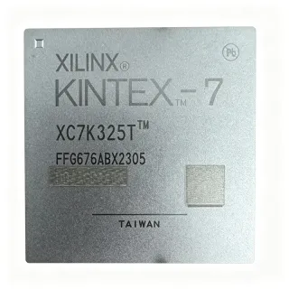
XC7K410T-1FFG676C - Kintex-7 FPGA 406K Logic Cells | AMD
MPN: XC7K410T-1FFG676C ✓ Active| Qty | Unit Price | Extended |
|---|---|---|
| 1 | $1051.9 | $1,051.90 |
| 10 | $998.5 | $9,985.00 |
| 100 | $945.2 | $94,520.00 |
| 500 | $892.8 | $446,400.00 |
| 1,000 | $840.5 | $840,500.00 |
XC7K410T-1FFG676C Overview
A Field Programmable Gate Array (FPGA) is an integrated circuit that can be configured by the customer or designer after manufacturing. Unlike fixed-function ASICs, FPGAs contain an array of programmable logic blocks and a hierarchy of reconfigurable interconnects that allow the blocks to be wired together in different configurations. This flexibility makes FPGAs ideal for prototyping, low-to-mid volume production, and applications requiring hardware reconfiguration. The Kintex-7 family sits between the Artix-7 (lowest cost) and Virtex-7 (highest performance) in AMD's 7-series portfolio, offering the best price/performance/watt at 28nm.
Key features of the XC7K410T-1FFG676C include 1,540 DSP48E1 slices for high-speed digital signal processing, 29.3 Mb of block RAM, and support for PCIe Gen3 x8 and 10 Gigabit Ethernet. The device operates from a 1.0V core voltage and supports a wide range of I/O standards including LVCMOS, LVDS, and HSTL. The -1 speed grade provides a balanced performance point suitable for many applications.
The architecture integrates configurable logic blocks (CLBs), block RAM, DSP slices, and high-speed transceivers. The 676-ball FCBGA package provides excellent thermal and electrical performance, with the exposed pad aiding heat dissipation. The device supports partial reconfiguration, allowing dynamic updates to specific logic regions without disrupting the entire design.
Typical applications include wired communications, broadcast, aerospace and defense, and high-performance computing. The high DSP ratio and cost-effective packaging make it particularly well-suited for wireless MIMO base stations, medical imaging, and video processing systems.
When designing with this device, careful attention must be paid to power supply decoupling and thermal management. The 1.0V core supply requires a robust power delivery network with multiple decoupling capacitors to maintain signal integrity at high switching frequencies.
Drop-in alternatives for XC7K410T-1FFG676C — same package, pin-to-pin compatible. Different-package parts requiring PCB rework are excluded.
Quick Comparison Tool — Select alternative parts for side-by-side comparison:
XC7K410T-2FFG676C
✅ Drop-In📋 Reference alternative (not in catalog)
XC7K410T-1FFG676I
✅ Drop-In📋 Reference alternative (not in catalog)
XC7K410T-2FFG676I
✅ Drop-In📋 Reference alternative (not in catalog)
XC7K325T-2FFG676C
✅ Drop-In📋 Reference alternative (not in catalog)
XC7K480T-2FFG676C
✅ Drop-In ⚠️ Specs Unverified📋 Reference alternative (not in catalog)
XC7K410T-1FFG676C Maximum Ratings & Electrical Characteristics
| Family | Kintex-7 |
| Logic Cells | 406720 |
| Number of I/O | 400 |
| Block RAM | 29306880 bits |
| DSP Slices | 1540 |
| Package | 676-BBGA, FCBGA |
| Technology | 28nm |
| Core Voltage | 1.0V |
| Speed Grade | -1 |
| Operating Temperature | 0C to +85C |
| Mounting Type | Surface Mount |
| Number of Terminals | 676 |
| Package Shape | Square |
| Terminal Form | Ball |
| RoHS Status | Compliant |
XC7K410T-1FFG676C Pin Configuration
| Pin A1 | IO_L1P_T0 — User I/O differential pair positive |
| Pin A2 | IO_L1N_T0 — User I/O differential pair negative |
| Pin B1 | VCCINT — Internal core voltage 1.0V |
| Pin B2 | GND — Ground |
| Pin C1 | IO_L2P_T0 — User I/O differential pair positive |
| Pin C2 | IO_L2N_T0 — User I/O differential pair negative |
| Pin D1 | VCCAUX — Auxiliary voltage 1.8V |
| Pin D2 | GND — Ground |
| Pin E1 | IO_L3P_T0 — User I/O differential pair positive |
| Pin E2 | IO_L3N_T0 — User I/O differential pair negative |
| Pin F1 | VCCBRAM — Block RAM voltage 1.0V |
| Pin F2 | GND — Ground |
Typical Applications
XC7K410T-1FFG676C is suitable for 6 applications: Wired Communications, Broadcast and Video Processing, Aerospace and Defense, High-Performance Computing, Medical Imaging, Wireless MIMO Base Stations.
Wired Communications
The XC7K410T-1FFG676C excels in wired communications equipment such as switches, routers, and line cards. Its 400 I/O pins and support for 10 Gigabit Ethernet enable high-speed data processing. The 1,540 DSP slices handle complex packet processing and traffic management algorithms. The 29.3 Mb of block RAM provides ample buffering for network queues. The -1 speed grade balances performance and power, making it suitable for cost-sensitive networking gear. Designers can implement flexible MAC and PHY layers, while the FPGA's reconfigurability allows protocol updates without hardware changes.
Recommended
Broadcast and Video Processing
In broadcast and video processing, the XC7K410T-1FFG676C provides the logic density and DSP capability needed for real-time video encoding, decoding, and format conversion. The 406,720 logic cells accommodate complex video pipelines, while the 1,540 DSP slices accelerate filtering and scaling operations. The 400 I/O pins interface with multiple video standards including SDI and HDMI. The 29.3 Mb block RAM supports line buffering and frame storage. The commercial temperature range suits studio environments. The FPGA's parallel processing architecture delivers the throughput required for 4K and 8K video streams.
Recommended
Aerospace and Defense
The XC7K410T-1FFG676C is well-suited for aerospace and defense applications such as radar, electronic warfare, and secure communications. Its 28nm technology provides high performance with manageable power consumption, critical for embedded systems. The 1,540 DSP slices enable sophisticated signal processing for radar beamforming and target detection. The 400 I/O pins interface with various sensors and data links. The FPGA's reconfigurability allows in-field updates for evolving mission requirements. The commercial temperature grade is suitable for many ground-based systems, while the -I variant supports extended temperature environments.
Recommended
High-Performance Computing
In high-performance computing, the XC7K410T-1FFG676C accelerates compute-intensive workloads through hardware parallelism. The 406,720 logic cells implement custom accelerators for scientific simulations, financial modeling, and data analytics. The 1,540 DSP slices provide high-throughput floating-point and fixed-point arithmetic. The 29.3 Mb block RAM supports local data caching, reducing external memory bandwidth demands. The 400 I/O pins connect to high-speed memory interfaces and interconnects. The -1 speed grade offers a balanced performance point for compute acceleration, while the FCBGA package ensures good thermal performance under sustained load.
Recommended
Medical Imaging
The XC7K410T-1FFG676C is ideal for medical imaging systems such as ultrasound, CT, and MRI. The 1,540 DSP slices accelerate image reconstruction and enhancement algorithms, while the 406,720 logic cells implement complex processing pipelines. The 400 I/O pins interface with high-speed ADCs and DACs. The 29.3 Mb block RAM supports image buffering and intermediate storage. The FPGA's parallel processing enables real-time imaging with low latency. The commercial temperature range suits clinical environments. The device's reconfigurability allows algorithm updates for new imaging modalities without hardware redesign.
Recommended
Wireless MIMO Base Stations
The XC7K410T-1FFG676C is well-suited for wireless MIMO base stations, offering high DSP ratios for beamforming and signal processing. The 1,540 DSP slices handle complex matrix operations for MIMO precoding and decoding. The 406,720 logic cells implement the baseband processing chain, including channel estimation and error correction. The 400 I/O pins connect to multiple RF transceivers. The 29.3 Mb block RAM supports buffering of multiple data streams. The -1 speed grade provides sufficient performance for LTE and 5G NR baseband processing while managing power consumption in remote radio heads.
Recommended
Recommended Products Summary
Engineering reference data for XC7K410T-1FFG676C — comparison, design guidance, and compliance information.
Selection Guide
Comparison with Alternatives
| Parameter | This Product | XC7K410T-2FFG676C | XC7K410T-1FFG676I | XC7K410T-2FFG676I | XC7K325T-2FFG676C | XC7K480T-2FFG676C |
|---|---|---|---|---|---|---|
| Package | 676-BBGA, FCBGA | 676-BBGA, FCBGA - same | 676-BBGA, FCBGA - same | 676-BBGA, FCBGA - same | 676-BBGA, FCBGA - same | 676-BBGA, FCBGA - same |
| Brand | AMD | AMD | AMD | AMD | AMD | AMD |
| Logic Cells | 406720 | 406720 | 406720 | 406720 | 326080 | 477760 |
| Number of I/O | 400 | 400 | 400 | 400 | 400 | 400 |
| Block RAM | 29306880 bits | 29306880 bits | 29306880 bits | 29306880 bits | 16020000 bits | 38304000 bits |
| DSP Slices | 1540 | 1540 | 1540 | 1540 | 840 | 1920 |
| Speed Grade | -1 | -2 | -1 | -2 | -2 | -2 |
| Operating Temperature | 0C to +85C | 0C to +85C | -40C to +100C | -40C to +100C | 0C to +85C | 0C to +85C |
Key Differentiators
- Higher logic density than XC7K325T (vs XC7K325T-2FFG676C)
- More DSP slices than XC7K325T (vs XC7K325T-2FFG676C)
- Lower cost than XC7K480T (vs XC7K480T-2FFG676C)
Design Notes
The XC7K410T-1FFG676C requires a robust power delivery network. The core voltage (VCCINT) is 1.0V and must be regulated tightly, typically within +/-3%. Use multiple low-ESR ceramic capacitors (0.1uF and 1uF) placed close to the VCCINT pins to handle transient currents. The auxiliary voltage (VCCAUX) is 1.8V and should be decoupled similarly. Refer to the AMD Kintex-7 power management application notes for detailed recommendations.
The 676-ball FCBGA package has an exposed pad that must be soldered to a thermal via array on the PCB for effective heat dissipation. The maximum junction temperature is 85C for the commercial grade. Calculate the power dissipation based on your design's logic utilization and clock frequency, then ensure the thermal resistance of your PCB and any heatsink keeps the junction temperature within limits. For high-utilization designs, consider forced-air cooling.
For high-speed serial transceivers and memory interfaces, maintain controlled impedance traces and minimize stub lengths. Use ground planes beneath all high-speed signal layers. The FCBGA package requires a fan-out pattern with microvias or blind vias for dense routing. Follow the AMD PCB design guidelines in UG483 for proper decoupling capacitor placement and power plane partitioning.
Compliance Information
RoHS compliance indicated by distributor listings. Other compliance data not explicitly provided in verified web data.