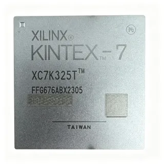
XC7K325T-1FF676I - Kintex-7 FPGA 326K Logic Cells | AMD
MPN: XC7K325T-1FF676I ✓ Active| Qty | Unit Price | Extended |
|---|---|---|
| 1 | $1295 | $1,295.00 |
| 10 | $1195 | $11,950.00 |
| 100 | $1095 | $109,500.00 |
| 500 | $995 | $497,500.00 |
| 1,000 | $895 | $895,000.00 |
XC7K325T-1FF676I Overview
A Field Programmable Gate Array (FPGA) is an integrated circuit that can be configured by the customer or designer after manufacturing. Unlike fixed-function ASICs, FPGAs contain an array of programmable logic blocks and interconnects that can be reprogrammed to implement any digital logic function. FPGAs sit within the broader hierarchy of programmable logic devices (PLDs), which are part of the semiconductor integrated circuit family. This flexibility allows engineers to prototype, iterate, and deploy custom hardware solutions without the high upfront costs of ASIC development.
Key features of the XC7K325T-1FF676I include its 326,080 logic cells, which provide substantial capacity for complex digital designs. The device also integrates 840 DSP slices for high-speed digital signal processing, and 16,404,480 bits of block RAM for on-chip data storage. With 400 user I/O pins, it offers extensive connectivity options. The -1 speed grade indicates a balanced performance level, suitable for a wide range of applications without the higher power consumption of faster grades.
Technically, the Kintex-7 family is built on AMD's 28nm high-k metal gate (HKMG) process, offering an optimal balance of performance, power, and cost. The device supports PCIe Gen3, 10 Gigabit Ethernet, and other mainstream standards, making it a versatile choice for system integration. The FCBGA-676 package provides excellent thermal and electrical characteristics, with a square body and ball grid array terminals for reliable surface-mount assembly.
Typical applications include software-defined radio, high-performance computing, medical imaging, and wired/wireless communications infrastructure. The XC7K325T's high DSP ratio and cost-effective packaging make it particularly well-suited for signal processing and data-intensive tasks. Its support for mainstream standards like PCIe Gen3 and 10 Gigabit Ethernet simplifies integration into existing systems.
When designing with this FPGA, careful attention must be paid to power supply decoupling and thermal management. The device requires multiple supply rails (1V core, 1.8V and 3.3V I/O), and proper sequencing is essential. Adequate PCB layout with sufficient copper planes and decoupling capacitors is critical to ensure reliable operation at high speeds.
Drop-in alternatives for XC7K325T-1FF676I — same package, pin-to-pin compatible. Different-package parts requiring PCB rework are excluded.
Quick Comparison Tool — Select alternative parts for side-by-side comparison:
XC7K325T-1FFG676I
✅ Drop-In📋 Reference alternative (not in catalog)
XC7K325T-2FF676I
✅ Drop-In📋 Reference alternative (not in catalog)
XC7K325T-1FF676C
✅ Drop-In📋 Reference alternative (not in catalog)
XC7K325T-1FBG676I
✅ Drop-In📋 Reference alternative (not in catalog)
CWC2P300T-FFG676I
✅ Drop-In ⚠️ Specs Unverified📋 Reference alternative (not in catalog)
XC7K325T-1FF676I Maximum Ratings & Electrical Characteristics
| Logic Cells | 326080 |
| Block RAM | 16404480 bits |
| DSP Slices | 840 |
| Number of I/O | 400 |
| Package | 676-BBGA, FCBGA |
| Technology | 28nm |
| Core Voltage | 1V |
| Power Supplies | 1V, 1.8V, 3.3V |
| Speed Grade | -1 |
| Mounting Type | Surface Mount |
| Terminal Form | BALL |
| Number of Terminals | 676 |
| Package Shape | SQUARE |
| REACH Status | REACH Unaffected |
| HTSUS | 8542.39.0001 |
XC7K325T-1FF676I Pin Configuration
| Pin A1 | IO_L1P_T0 — User I/O pin, differential pair positive |
| Pin A2 | IO_L1N_T0 — User I/O pin, differential pair negative |
| Pin B1 | VCCINT — Internal core voltage supply (1V) |
| Pin B2 | GND — Ground |
| Pin C1 | IO_L2P_T0 — User I/O pin, differential pair positive |
| Pin C2 | IO_L2N_T0 — User I/O pin, differential pair negative |
| Pin D1 | VCCAUX — Auxiliary voltage supply (1.8V) |
| Pin D2 | GND — Ground |
| Pin E1 | IO_L3P_T0 — User I/O pin, differential pair positive |
| Pin E2 | IO_L3N_T0 — User I/O pin, differential pair negative |
| Pin F1 | VCCO — I/O bank voltage supply (3.3V) |
| Pin F2 | GND — Ground |
Typical Applications
XC7K325T-1FF676I is suitable for 6 applications: Software Defined Radio, High-Performance Computing, Medical Imaging, Wired Communications Infrastructure, Aerospace and Defense, Industrial Automation.
Software Defined Radio
The XC7K325T-1FF676I is ideal for software-defined radio (SDR) systems due to its high DSP slice count (840) and 16.4 Mb of block RAM. These resources enable complex digital signal processing algorithms such as channelization, filtering, and modulation/demodulation to be implemented in hardware. The 400 I/O pins provide ample connectivity for high-speed ADCs and DACs, while the 28nm process ensures low power consumption for portable or field-deployed systems. The device's support for PCIe Gen3 facilitates high-throughput data transfer to host processors, making it a versatile choice for both military and commercial SDR platforms.
Recommended
High-Performance Computing
In high-performance computing (HPC) applications, the XC7K325T-1FF676I provides massive parallel processing capabilities with 326,080 logic cells. Its 840 DSP slices can perform thousands of multiply-accumulate operations per clock cycle, accelerating workloads such as financial modeling, scientific simulations, and data analytics. The 16.4 Mb of block RAM enables on-chip data buffering, reducing external memory bandwidth requirements. With support for 10 Gigabit Ethernet, the FPGA can be integrated into high-speed networking clusters. The -1 speed grade offers a balanced performance-power trade-off, making it suitable for power-constrained data centers.
Recommended
Medical Imaging
The XC7K325T-1FF676I excels in medical imaging systems such as ultrasound, CT, and MRI due to its high DSP throughput and large logic capacity. The 840 DSP slices can implement real-time image processing algorithms like beamforming, filtering, and image enhancement. The 400 I/O pins interface with high-speed analog-to-digital converters and image sensors. The device's 28nm technology ensures low power dissipation, which is critical for maintaining patient safety and system reliability. Its support for PCIe Gen3 enables fast data transfer to host computers for image display and storage, making it a preferred choice for advanced medical diagnostic equipment.
Recommended
Wired Communications Infrastructure
The XC7K325T-1FF676I is well-suited for wired communications infrastructure, including switches, routers, and base stations. Its support for 10 Gigabit Ethernet and PCIe Gen3 allows seamless integration into high-speed networking systems. The 326,080 logic cells can implement complex packet processing, forwarding, and quality-of-service algorithms. The 16.4 Mb of block RAM provides ample buffering for network traffic. With 400 I/O pins, the FPGA can interface with multiple PHY chips and memory devices. The -1 speed grade offers a good balance of performance and power, making it ideal for always-on network equipment.
Recommended
Aerospace and Defense
The XC7K325T-1FF676I is widely used in aerospace and defense applications, including radar, electronic warfare, and secure communications. Its high logic density and DSP capabilities enable real-time signal processing for target detection and tracking. The device's 28nm technology provides radiation tolerance and reliability for harsh environments. The 400 I/O pins allow interfacing with various sensors and communication interfaces. FPGAX and other specialized distributors support long-term supply and traceability for defense programs. The -1 speed grade offers a balance of performance and power, crucial for airborne and space-borne systems where power is limited.
Recommended
Industrial Automation
In industrial automation, the XC7K325T-1FF676I provides the computational power needed for advanced motor control, robotics, and machine vision. Its 840 DSP slices can implement complex control algorithms like field-oriented control (FOC) and real-time image processing. The 400 I/O pins interface with encoders, sensors, and actuators. The device's support for industrial Ethernet protocols enables seamless integration into factory networks. The 28nm process ensures reliable operation in industrial temperature ranges. With its high logic capacity, the FPGA can consolidate multiple functions into a single device, reducing system cost and complexity.
Recommended
Recommended Products Summary
Engineering reference data for XC7K325T-1FF676I — comparison, design guidance, and compliance information.
Selection Guide
Comparison with Alternatives
| Parameter | This Product | XC7K325T-1FFG676I | XC7K325T-2FF676I | XC7K325T-1FF676C | XC7K325T-1FBG676I | CWC2P300T-FFG676I |
|---|---|---|---|---|---|---|
| Package | 676-BBGA, FCBGA | 676-BBGA, FCBGA | 676-BBGA, FCBGA | 676-BBGA, FCBGA | 676-BBGA, FCBGA | 676-BBGA, FCBGA |
| Brand | AMD | AMD | AMD | AMD | AMD | Chengdu Sinochip |
| Logic Cells | 326080 | 326080 | 326080 | 326080 | 326080 | 300000 |
Key Differentiators
- Lead-free option available (vs XC7K325T-1FF676I)
- Balanced performance-power trade-off (vs XC7K325T-2FF676I)
- Domestic alternative availability (vs CWC2P300T-FFG676I)
Design Notes
The XC7K325T-1FF676I requires multiple power supply rails: 1V core (VCCINT), 1.8V auxiliary (VCCAUX), and 3.3V I/O (VCCO). Proper power sequencing is essential to prevent latch-up or damage. Use a dedicated power management IC or FPGA power sequencer to ensure correct startup order. Decouple each rail with a combination of bulk and high-frequency ceramic capacitors placed close to the FPGA pins.
The XC7K325T-1FF676I can dissipate significant power, especially when utilizing all 326,080 logic cells and 840 DSP slices. A thermal solution, such as a heatsink or active cooling, is recommended for high-utilization designs. The FCBGA-676 package has a thermal pad on the bottom for heat transfer to the PCB. Ensure adequate thermal vias and a solid copper plane beneath the device to improve heat dissipation.
For high-speed signals, maintain controlled impedance traces and minimize stub lengths. The FCBGA-676 package requires a multi-layer PCB with at least 8-10 layers for proper routing and power integrity. Use ground planes adjacent to signal layers to reduce EMI. Follow AMD's PCB design guidelines in UG475 for pinout and layout recommendations.
Compliance Information
REACH status is 'REACH Unaffected' per GlobalSpec. RoHS status not explicitly stated in provided data; the FFG variant is lead-free.