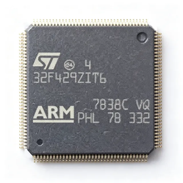
STM32F429ZIT6 - 2MB Flash 180MHz Cortex-M4 MCU | STMicroelectronics
N.º da peça: STM32F429ZIT6 ✓ Ativo| Qtd. | Preço unitário | Total |
|---|---|---|
| 1 | $18.75 | $18,75 |
| 10 | $16.95 | $169,50 |
| 100 | $14.2 | $1.420,00 |
| 500 | $12.85 | $6.425,00 |
| 1.000 | $11.4 | $11.400,00 |
STM32F429ZIT6 Visão geral
What is a microcontroller? A microcontroller (MCU) is a compact integrated circuit that governs a specific operation in an embedded system, combining a processor core, flash memory, SRAM, and programmable peripherals on a single chip. The STM32F429ZIT6 sits within the STM32F4 series, part of the broader STM32 family of 32-bit ARM Cortex-M microcontrollers, which in turn belongs to the general hierarchy of embedded processors and system-on-chip devices used across industrial, consumer, and IoT applications.
Key features include the ARM Cortex-M4 core with single-precision FPU and DSP instructions, ART Accelerator enabling 0-wait-state execution from flash, and 225 DMIPS (1.25 DMIPS/MHz at 180 MHz). Memory resources total 2 MB of flash and 256 KB of system SRAM plus 4 KB of backup SRAM. Peripheral integration is extensive: three 12-bit ADCs, two DACs, 12 general-purpose 16-bit timers plus two 32-bit timers, multiple USART/SPI/I2C interfaces, USB OTG full-speed and high-speed, 10/100 Ethernet MAC, and a TFT-LCD parallel interface (8080/6800) that supports up to XGA resolution. Supply voltage range is 1.8V to 3.6V (3.3V typical).
Architecturally, the adaptive real-time (ART) accelerator pairs with the dual-bank flash organization to support read-while-write operation, which is critical for in-field or over-the-air firmware updates. Clock generation supports an external crystal and internal RC sources feeding a PLL that synthesizes the 180 MHz system clock, while a memory protection unit (MPU) supports robust RTOS partitioning and a cryptographic/hash engine (on related F4 variants) provides hardware acceleration for security workloads.
Typical applications include industrial control and automation, HMI panels with TFT displays, motor drives, IoT gateways using Ethernet, and medical instrumentation where real-time control and rich connectivity are required. The device is also widely used in audio processing thanks to its DSP extensions and I2S peripherals, and in graphical user interfaces via the integrated LCD-TFT controller.
Design consideration: decouple every VDD pin with 100 nF X7R capacitors placed close to the pins, add a 4.7 uF bulk capacitor near the regulator, and filter the VDDA analog supply with a ferrite bead plus 10 nF + 1 uF decoupling; budget PCB copper area for thermal dissipation in high-load designs where the MCU draws sustained currents above 100 mA.
This page synthesizes distributor availability, same-package drop-in alternatives, and practical design notes not found in the STMicroelectronics datasheet, giving engineers a complete evaluation resource.
Alternativas drop-in para STM32F429ZIT6 — mesmo encapsulamento, compatível pino a pino. Peças de encapsulamento diferente que exigem retrabalho na PCB são excluídas.
Variantes desta série
Modelos da mesma série compatíveis como drop-in com STM32F429ZIT6 (mesmo formato e footprint) — diferindo em Package, Core, Operating Temperature, Timers, SRAM.
Ferramenta de comparação rápida — selecione peças alternativas para comparação lado a lado:
STM32F429ZET6
✅ Drop-In✓ Em estoque
Consulte o preço
Ver ficha técnica →STM32F427ZIT6
✅ Drop-In✓ Em estoque
$8.1 / unidade
Ver ficha técnica →STM32F429ZGT6
✅ Drop-In✓ Em estoque
$10.95 / unidade
Ver ficha técnica →STM32F469ZIT6
✅ Drop-In✓ Em estoque
$17.83 / unidade
Ver ficha técnica →STM32F437IIH6
✅ Drop-In✓ Em estoque
$10.6 / unidade
Ver ficha técnica →STM32F429IIT6
✅ Drop-In✓ Em estoque
$8.3523 / unidade
Ver ficha técnica →STM32F429ZIT6 Classificações máximas e características elétricas
| Core | ARM Cortex-M4 with FPU and DSP |
| Frequência máxima de clock | 180 MHz |
| Program Memory (Flash) | 2 MB |
| Data RAM | 256 KB SRAM + 4 KB backup SRAM |
| Largura do barramento de dados | 32 bit |
| Performance | 225 DMIPS (1.25 DMIPS/MHz) |
| Supply Voltage Range | 1.8 V to 3.6 V |
| Faixa de temperatura de operação | -40C to +85C |
| Encapsulamento | LQFP-144 (20 x 20 mm) |
| Tipo de montagem | Surface Mount (SMD/SMT) |
| ADC | 3x 12-bit, up to 2.4 MSPS |
| DAC | 2x 12-bit |
| Timers | 12x 16-bit + 2x 32-bit (17 timers total) |
| Communication Interfaces | USB OTG HS/FS, 10/100 Ethernet, USART/UART, SPI, I2C, CAN, I2S, SAI, UART |
| LCD-TFT Controller | Yes, parallel 8080/6800, up to XGA |
| Camera Interface | 8-14 bit parallel |
| Status RoHS | Compliant |
| Cryptographic Acceleration | Yes (AES, hash, RNG on F4 series) |
Configuração de pinos do STM32F429ZIT6
| Pino 1 | PE2 — GPIO, TRACECLK |
| Pino 2 | PE3 — GPIO, TRACED0 |
| Pino 3 | PE4 — GPIO, TRACED1 |
| Pino 4 | PE5 — GPIO, TRACED2 |
| Pino 5 | PE6 — GPIO, TRACED3 |
| Pino 6 | VBAT — Backup battery supply |
| Pino 7 | PC13 — GPIO, RTC_TAMP1 |
| Pino 8 | PC14 — GPIO, OSC32_IN |
| Pino 9 | PC15 — GPIO, OSC32_OUT |
| Pino 10 | VREF+ — ADC reference voltage |
| Pino 11 | VDDA — Analog supply voltage |
| Pino 12 | PA0 — GPIO, UART4_TX, ADC1_IN0 |
| Pino 13 | PA1 — GPIO, UART4_RX, ADC1_IN1 |
| Pino 14 | PA2 — GPIO, USART2_TX, ADC1_IN2 |
| Pino 15 | PA3 — GPIO, USART2_RX, ADC1_IN3 |
| Pino 16 | PA4 — GPIO, SPI1_NSS, ADC1_IN4, DAC1_OUT |
| Pino 17 | PA5 — GPIO, SPI1_SCK, ADC1_IN5, DAC2_OUT |
| Pino 18 | PA6 — GPIO, SPI1_MISO, ADC1_IN6 |
| Pino 19 | PA7 — GPIO, SPI1_MOSI, ADC1_IN7 |
| Pino 20 | PC4 — GPIO, ADC2_IN14 |
| Pino 21 | PC5 — GPIO, ADC2_IN15 |
| Pino 22 | PB0 — GPIO, ADC3_IN8, TIM3_CH3 |
| Pino 23 | PB1 — GPIO, ADC3_IN9, TIM3_CH4 |
| Pino 24 | PB2 — GPIO, BOOT1 |
| Pino 25 | PE7 — GPIO |
| Pino 26 | PE8 — GPIO |
| Pino 27 | PE9 — GPIO |
| Pino 28 | PE10 — GPIO |
| Pino 29 | PE11 — GPIO |
| Pino 30 | PE12 — GPIO |
| Pino 31 | PE13 — GPIO |
| Pino 32 | PE14 — GPIO |
| Pino 33 | PE15 — GPIO |
| Pino 34 | PB10 — GPIO, I2C2_SCL, USART3_TX |
| Pino 35 | PB11 — GPIO, I2C2_SDA, USART3_RX |
| Pino 36 | VCAP_1 — Core regulator bypass |
| Pino 37 | VDD — Digital supply voltage |
| Pino 38 | VSS — Digital ground |
| Pino 39 | PB12 — GPIO, SPI2_NSS, CAN2_RX |
| Pino 40 | PB13 — GPIO, SPI2_SCK, CAN2_TX |
| Pino 41 | PB14 — GPIO, SPI2_MISO, TIM12_CH1 |
| Pino 42 | PB15 — GPIO, SPI2_MOSI, TIM12_CH2 |
| Pino 43 | PD8 — GPIO, USART3_TX |
| Pino 44 | PD9 — GPIO, USART3_RX |
| Pino 45 | PD10 — GPIO |
| Pino 46 | PD11 — GPIO |
| Pino 47 | PD12 — GPIO, TIM4_CH1 |
| Pino 48 | PD13 — GPIO, TIM4_CH2 |
| Pino 49 | PD14 — GPIO, TIM4_CH3 |
| Pino 50 | PD15 — GPIO, TIM4_CH4 |
| Pino 51 | PC6 — GPIO, USART6_TX, TIM3_CH1 |
| Pino 52 | PC7 — GPIO, USART6_RX, TIM3_CH2 |
| Pino 53 | PC8 — GPIO, TIM3_CH3, SDMMC1_D0 |
| Pino 54 | PC9 — GPIO, TIM3_CH4, SDMMC1_D1 |
| Pino 55 | PA8 — GPIO, TIM1_CH1, MCO1 |
| Pino 56 | PA9 — GPIO, USART1_TX, TIM1_CH2 |
| Pino 57 | PA10 — GPIO, USART1_RX, TIM1_CH3 |
| Pino 58 | PA11 — GPIO, USB OTG D-, CAN1_RX |
| Pino 59 | PA12 — GPIO, USB OTG D+, CAN1_TX |
| Pino 60 | PA13 — GPIO, JTMS-SWDIO |
| Pino 61 | VCAP_2 — Core regulator bypass |
| Pino 62 | VDD — Digital supply voltage |
| Pino 63 | VSS — Digital ground |
| Pino 64 | PA14 — GPIO, JTCK-SWCLK |
| Pino 65 | PA15 — GPIO, JTDI, SPI3_NSS |
| Pino 66 | PC10 — GPIO, UART4_TX, SDMMC1_D2 |
| Pino 67 | PC11 — GPIO, UART4_RX, SDMMC1_D3 |
| Pino 68 | PC12 — GPIO, UART5_TX, SDMMC1_CK |
| Pino 69 | PD0 — GPIO, CAN1_RX |
| Pino 70 | PD1 — GPIO, CAN1_TX |
| Pino 71 | PD2 — GPIO, SDMMC1_CMD |
| Pino 72 | PD3 — GPIO, USART2_CTS |
| Pino 73 | PD4 — GPIO, USART2_RTS |
| Pino 74 | PD5 — GPIO, USART2_TX |
| Pino 75 | PD6 — GPIO, USART2_RX |
| Pino 76 | PD7 — GPIO, USART2_CK |
| Pino 77 | PB3 — GPIO, JTDO-TRACESWO, TIM2_CH2 |
| Pino 78 | PB4 — GPIO, NJTRST, TIM3_CH1 |
| Pino 79 | PB5 — GPIO, I2C1_SMBAI |
| Pino 80 | PB6 — GPIO, I2C1_SCL, USART1_TX |
| Pino 81 | PB7 — GPIO, I2C1_SDA, USART1_RX |
| Pino 82 | BOOT0 — Boot mode select |
| Pino 83 | PB8 — GPIO, I2C1_SCL, CAN1_RX |
| Pino 84 | PB9 — GPIO, I2C1_SDA, CAN1_TX |
| Pino 85 | PE0 — GPIO, TIM4_ETR |
| Pino 86 | PE1 — GPIO |
| Pino 87 | VCAP_3 — Core regulator bypass |
| Pino 88 | VDD — Digital supply voltage |
| Pino 89 | VSS — Digital ground |
| Pino 90 | PF0 — GPIO, I2C2_SDA |
| Pino 91 | PF1 — GPIO, I2C2_SCL |
| Pino 92 | PF2 — GPIO |
| Pino 93 | PF3 — GPIO |
| Pino 94 | PF4 — GPIO |
| Pino 95 | PF5 — GPIO |
| Pino 96 | VSS — Digital ground |
| Pino 97 | VSS — Digital ground |
| Pino 98 | PF6 — GPIO, TIM10_CH1 |
| Pino 99 | PF7 — GPIO, TIM11_CH1 |
| Pino 100 | PF8 — GPIO |
| Pino 101 | PF9 — GPIO |
| Pino 102 | PF10 — GPIO |
| Pino 103 | PF11 — GPIO |
| Pino 104 | PF12 — GPIO |
| Pino 105 | PF13 — GPIO |
| Pino 106 | PF14 — GPIO |
| Pino 107 | PF15 — GPIO |
| Pino 108 | PG0 — GPIO |
| Pino 109 | PG1 — GPIO |
| Pino 110 | PE2 — GPIO, TRACECLK |
| Pino 111 | PE3 — GPIO, TRACED0 |
| Pino 112 | PE4 — GPIO, TRACED1 |
| Pino 113 | PE5 — GPIO, TRACED2 |
| Pino 114 | PE6 — GPIO, TRACED3 |
| Pino 115 | VSS — Digital ground |
| Pino 116 | PG2 — GPIO |
| Pino 117 | PG3 — GPIO |
| Pino 118 | PG4 — GPIO |
| Pino 119 | PG5 — GPIO |
| Pino 120 | PG6 — GPIO |
| Pino 121 | PG7 — GPIO |
| Pino 122 | PG8 — GPIO |
| Pino 123 | VSS — Digital ground |
| Pino 124 | VDD — Digital supply voltage |
| Pino 125 | PG9 — GPIO, USART6_RX |
| Pino 126 | PG10 — GPIO |
| Pino 127 | PG11 — GPIO, SDMMC2_D2 |
| Pino 128 | PG12 — GPIO, SDMMC2_D3 |
| Pino 129 | PG13 — GPIO, SDMMC2_CK |
| Pino 130 | PG14 — GPIO, SDMMC2_CMD |
| Pino 131 | PG15 — GPIO |
| Pino 132 | PB6 — GPIO, I2C1_SCL |
| Pino 133 | PB7 — GPIO, I2C1_SDA |
| Pino 134 | PB8 — GPIO, I2C1_SCL, CAN1_RX |
| Pino 135 | PB9 — GPIO, I2C1_SDA, CAN1_TX |
| Pino 136 | PC8 — GPIO |
| Pino 137 | PC9 — GPIO |
| Pino 138 | NRST — Reset input (active low) |
| Pino 139 | PA0 — GPIO, WKUP, ADC1_IN0 |
| Pino 140 | PA1 — GPIO, ADC1_IN1 |
| Pino 141 | PA2 — GPIO, USART2_TX |
| Pino 142 | PA3 — GPIO, USART2_RX |
| Pino 143 | VSS — Digital ground |
| Pino 144 | VDD — Digital supply voltage |
Aplicações típicas
STM32F429ZIT6 é adequado para 7 aplicaçãos: Industrial TFT HMI Panels, Industrial Motor Drives, IoT Ethernet Gateways, Audio Processing and DSP, Medical Instrumentation, Camera and Vision Systems, Smart Home Hubs.
Industrial TFT HMI Panels
The STM32F429ZIT6 is purpose-built for industrial HMI displays thanks to its integrated parallel 8080/6800 LCD-TFT controller that supports up to XGA resolution without an external graphics chip. The 2 MB dual-bank flash and 256 KB SRAM hold WQVGA-frame buffers, font assets, and MODBUS/TCP stacks simultaneously. Its 225 DMIPS performance lets the same MCU drive the panel, run the HMI logic, and handle capacitive touch scanning, reducing the BOM. Reference design examples include washing machine panels and HVAC thermostats documented in ST application note AN4861.
Recomendado
Industrial Motor Drives
With 12 16-bit timers plus 2 32-bit timers, three 12-bit ADCs running up to 2.4 MSPS, and the 180 MHz Cortex-M4 with DSP instructions, the STM32F429ZIT6 is a strong fit for Field-Oriented Control (FOC) of three-phase PMSM and BLDC motors. The HRTIM timer and quadrature encoder inputs allow deterministic switching up to 100 kHz, while the FPU speeds up the Park/Clarke transforms required for sensorless control. Typical designs run the MCU at 24V bus with NUCLEO-F429ZI reference firmware from STM32CubeIDE as the starting point.
Recomendado
IoT Ethernet Gateways
The integrated 10/100 Ethernet MAC (with MII/RMII PHY interface) plus USB OTG HS/FS make the STM32F429ZIT6 a one-chip gateway for industrial IoT nodes bridging Modbus, BACnet, or PROFINET to cloud MQTT pipelines. The 2 MB flash accommodates full TLS stacks and OTA staging buffers, while the ART accelerator keeps interrupt latency under 12 cycles even with encryption on. Real-world designs pair it with an external PHY and a W5500 hardwired TCP/IP offload for redundant network paths.
Recomendado
Audio Processing and DSP
The Cortex-M4 with single-precision FPU and DSP instructions (MAC, SIMD) lets the STM32F429ZIT6 perform real-time audio processing for products like hearing aids, intercoms, and pro-audio effect units. Dual SAI/I2S peripherals handle up to four stereo codecs simultaneously, while the 256 KB SRAM is sufficient for 16-bit 48 kHz buffers across several channels. ST's audio library (AN4826) provides ready-made MP3, AAC, and FLAC decoders that fit inside the 2 MB flash with room for application code.
Recomendado
Medical Instrumentation
In medical designs such as patient monitors, infusion pumps, and portable diagnostics, the STM32F429ZIT6 provides 225 DMIPS for real-time DSP (ECG/EEG/PPG filtering) plus the safety features required by IEC 62304. Its three 12-bit ADCs sample sensor channels concurrently with hardware oversampling; the MPU and watchdog timers enable robust RTOS partitioning (FreeRTOS runs comfortably with 64 KB task stacks). Designs targeting FDA submission pair it with isolated communication transceivers.
Recomendado
Camera and Vision Systems
The integrated 8-14 bit parallel camera interface plus DCMI peripheral allows the STM32F429ZIT6 to ingest raw Bayer streams from OV5640 or similar CMOS sensors at up to WVGA resolution. Combined with the LCD-TFT controller, the same MCU both captures and displays images - a common pattern in barcode readers, low-cost machine-vision kiosks, and entry-level smart-home cameras. JPEG encoding is handled in software using the STM32 hardware JPEG codec offload.
Recomendado
Smart Home Hubs
In smart-home gateways that aggregate Zigbee, BLE, and Wi-Fi devices, the STM32F429ZIT6 serves as the central controller running the protocol stacks, rule engine, and TFT-driven touchscreen UI. The 2 MB flash stores OTA staging, TLS certificates, and font assets, while the 256 KB SRAM accommodates packet queues. USB OTG HS provides local docking for firmware updates via mass storage; Ethernet gives the wired backhaul to the home router.
Recomendado
Resumo dos produtos recomendados
Dados de referência de engenharia para STM32F429ZIT6 — comparação, orientação de projeto e informações de conformidade.
Guia de seleção
Comparação com alternativas
| Parâmetro | Este produto | STM32F429ZET6 | STM32F427ZIT6 | STM32F429ZGT6 | STM32F469ZIT6 | STM32F437IIH6 | STM32F429IIT6 |
|---|---|---|---|---|---|---|---|
| Brand | STMicroelectronics | STMicroelectronics | STMicroelectronics | STMicroelectronics | STMicroelectronics | STMicroelectronics | STMicroelectronics |
| Package | LQFP-144 | LQFP-144 - same | LQFP-144 - same | LQFP-144 - same | LQFP-144 - same | LQFP-144 - same | LQFP-176 - different |
| Core | ARM Cortex-M4 FPU | ARM Cortex-M4 FPU | ARM Cortex-M4 FPU | ARM Cortex-M4 FPU | ARM Cortex-M4 FPU + Chrom-ART | ARM Cortex-M4 FPU | ARM Cortex-M4 FPU |
| Maximum Clock Frequency | 180 MHz | 180 MHz | 180 MHz | 180 MHz | 180 MHz | 180 MHz | 180 MHz |
| Flash Memory | 2 MB | 512 KB | 2 MB | 1 MB | 2 MB | 2 MB | 2 MB |
| SRAM | 256 KB + 4 KB backup | 192 KB + 4 KB backup | 256 KB + 4 KB backup | 192 KB + 4 KB backup | 256 KB + 4 KB backup | 256 KB + 4 KB backup | 256 KB + 4 KB backup |
| LCD-TFT Controller | Yes | Yes | No | Yes | Yes (MIPI-DSI) | No | Yes |
| USB OTG | HS + FS | HS + FS | HS + FS | HS + FS | HS + FS | HS + FS | HS + FS |
| Ethernet MAC | 10/100 MAC | 10/100 MAC | 10/100 MAC | 10/100 MAC | 10/100 MAC | 10/100 MAC | 10/100 MAC |
| Cryptographic Acceleration | AES, hash, RNG | AES, hash, RNG | AES, hash, RNG | AES, hash, RNG | AES, hash, RNG | AES, hash, RNG | AES, hash, RNG |
Principais diferenciais
- Highest flash density in the F429 family in LQFP-144 (vs STM32F429ZET6)
- Integrated LCD-TFT parallel controller for HMI (vs STM32F427ZIT6)
- 4x SRAM versus ZGT6 variant in same package (vs STM32F429ZGT6)
- Chrom-ART accelerator for 2D GUI effects (vs STM32F469ZIT6)
Notas de projeto
Decouple every VDD pin with a 100 nF X7R ceramic capacitor placed within 5 mm of the pin, plus a shared 4.7 uF bulk capacitor on the 3.3V regulator output. The VDDA analog supply requires an additional ferrite bead plus 10 nF + 1 uF decoupling to keep ADC readings clean. For battery-backed designs, VBAT must have its own dedicated rail with a 100 nF cap; avoid loading the backup domain with more than a few microamps. Estimated total bypass budget is approximately 7-9 capacitors for a typical 144-pin design.
At 180 MHz with all peripherals active, the STM32F429ZIT6 draws approximately 50-60 mA from VDD, dissipating 165-200 mW. LQFP-144 has a typical theta_JA of 50 C/W on a 4-layer PCB, which yields a 25-30 C junction temperature rise - well within the 85 C industrial limit. For sustained full-load designs (motor control or HMI backlight), add a copper pour under the exposed thermal pad area on the top layer to keep Tj below 70 C.
Route the parallel LCD-TFT bus (D0-D15, HSYNC, VSYNC, DE, CLK) as a length-matched group with 50 ohm controlled impedance, keeping each trace within 100 mil of its neighbour. Separate the analog section (VDDA, VREF+, ADC inputs) on its own ground island connected to the main ground at a single point. Keep the HSE crystal traces short and symmetric, with the load capacitors placed within 2 mm of the OSC_IN/OSC_OUT pins.
Do not skip the VCAP pins - each must have its own 2.2 uF capacitor to ground, otherwise the internal 1.2V regulator will fail to start, producing seemingly dead boards. The BOOT0 pin must be pulled low through 10 kohm at reset for normal flash boot; pulling it high forces system memory bootloaders. NRST must be pulled up with 40 kohm internal plus optional external 10 kohm for noisy industrial environments.
For USB OTG HS operation at 480 Mbps, the D+/D- traces must be 90 ohm differential, length-matched to within 1 mm, and routed over a continuous ground reference. The USB DP/DM series resistors (typically 22 ohm) should be placed as close to the MCU as possible. For Ethernet MII/RMII, the 50 MHz clock trace length must be matched within 10 mm of the data lines to avoid setup/hold violations at 100 Mbps.
Informações de conformidade
RoHS compliant per ST product page. Industrial-grade -40C to +85C, not AEC-Q100 qualified for automotive; for automotive designs use the STM32F429ZIT6-Y variant or screen specifically qualified parts.