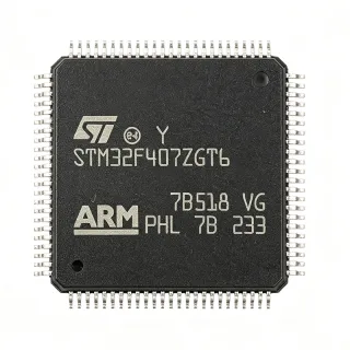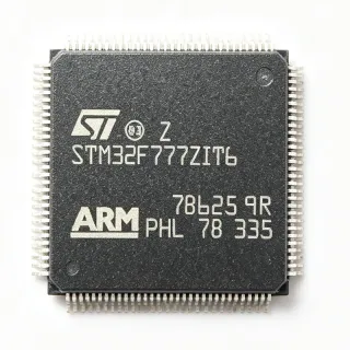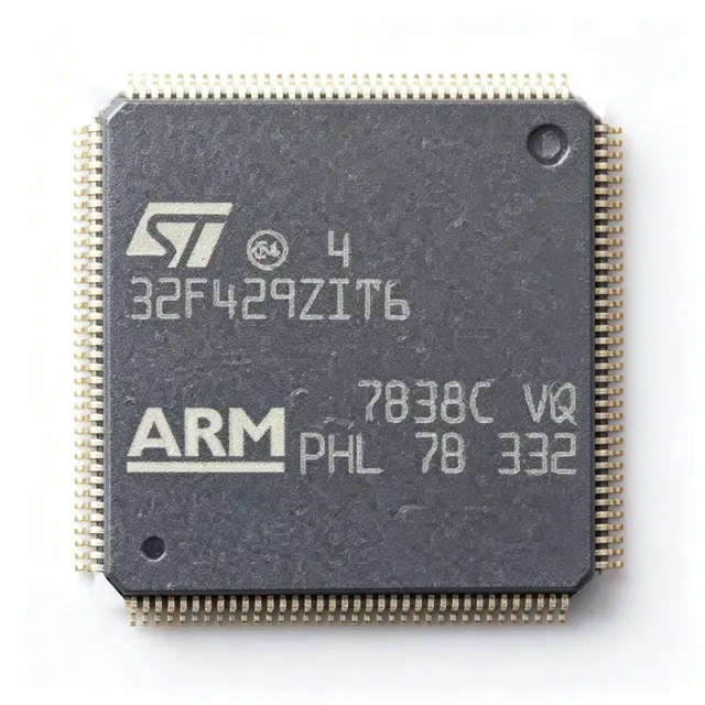
STM32F429ZIT6 - 2MB Flash 180MHz Cortex-M4 MCU | STMicroelectronics
MPN: STM32F429ZIT6 ✓ Active| Qty | Unit Price | Extended |
|---|---|---|
| 1 | $14.2 | $14.20 |
| 10 | $12.85 | $128.50 |
| 100 | $11.4 | $1,140.00 |
| 500 | $10.65 | $5,325.00 |
| 1,000 | $9.9 | $9,900.00 |
STM32F429ZIT6 Overview
What is a microcontroller? A microcontroller (MCU) is a compact integrated circuit that governs a specific operation in an embedded system, combining a processor core, flash memory, SRAM, and programmable peripherals on a single chip. The STM32F429ZIT6 sits within the STM32F4 series, part of the broader STM32 family of 32-bit ARM Cortex-M microcontrollers, which in turn belongs to the general hierarchy of embedded processors and system-on-chip devices.
Key features include the ARM Cortex-M4 core with single-precision FPU, DSP instructions, and ART Accelerator enabling 0-wait-state execution from flash, delivering 225 DMIPS (1.25 DMIPS/MHz at 180 MHz). Memory resources total 2 MB of flash and 256 KB of system SRAM plus 4 KB of backup SRAM. Peripheral integration is extensive: 12-bit ADCs, DACs, general-purpose and advanced timers, multiple USART/SPI/I2C interfaces, USB OTG, Ethernet MAC, and a TFT-LCD parallel interface (8080/6800). Supply voltage is 2.5V/3.3V class (1.8V to 3.6V range per ST documentation).
Architecturally, the adaptive real-time (ART) accelerator pairs with the dual-bank flash organization to support read-while-write operation, which is critical for in-field or over-the-air firmware updates. Clock generation supports an external crystal and internal RC sources feeding a PLL that synthesizes the 180 MHz system clock, while a memory protection unit (MPU) supports robust RTOS partitioning.
Typical applications include industrial control and automation, HMI panels with TFT displays, motor drives, IoT gateways using Ethernet, and medical instrumentation where real-time control and rich connectivity are required.
Design consideration: decouple every VDD pin with 100 nF capacitors placed close to the pins, add a 4.7 uF bulk capacitor, and filter the VDDA analog supply with a ferrite bead; budget PCB copper area for thermal dissipation in high-load designs.
This page synthesizes distributor availability, same-package drop-in alternatives, and practical design notes not found in the STMicroelectronics datasheet, giving engineers a complete evaluation resource.
Drop-in alternatives for STM32F429ZIT6 — same package, pin-to-pin compatible. Different-package parts requiring PCB rework are excluded.
Variants in this series
Same-series models that are drop-in compatible with STM32F429ZIT6 (same form factor and footprint) — differing in Flash Memory, SRAM, Core, Supply Voltage, Timers.
Quick Comparison Tool — Select alternative parts for side-by-side comparison:
STM32F415ZGT6
✅ Drop-In ⚠️ 参数待验证✓ In Stock
$8.5 / Unit
View Datasheet →STM32F446ZET6
✅ Drop-In ⚠️ 参数待验证✓ In Stock
$6.0455 / Unit
View Datasheet →STM32F723ZET6
✅ Drop-In ⚠️ 参数待验证✓ In Stock
$8.1 / Unit
View Datasheet →STM32F207ZET6
✅ Drop-In ⚠️ 参数待验证✓ In Stock
$8.1 / Unit
View Datasheet →STM32F103ZET6
✅ Drop-In ⚠️ 参数待验证✓ In Stock
$4.48 / Unit
View Datasheet →STM32F429ZIT6 Maximum Ratings & Electrical Characteristics
| Core | ARM 32-bit Cortex-M4 with FPU |
| Maximum Clock Frequency | 180 MHz |
| Performance | 225 DMIPS (1.25 DMIPS/MHz) |
| Flash Memory | 2 MB (2M x 8) |
| SRAM | 256 KB system + 4 KB backup |
| Data Bus Width | 32 bit |
| Core Architecture | ARM Cortex-M4 with DSP instructions and ART Accelerator |
| Supply Voltage | 2.5 V / 3.3 V (1.8 V to 3.6 V range) |
| Package / Case | LQFP-144 (20x20 mm) |
| Mounting Style | SMD/SMT |
| Peripherals | LCD parallel interface (8080/6800), DMA, USB OTG, Ethernet MAC |
| Memory Protection Unit | Yes (MPU) |
| Series | STM32F4 |
| I/O Pins | 114 GPIO (typical for LQFP144 ZI variant) |
| RoHS Status | Compliant |
STM32F429ZIT6 lqfp-144 (20x20 mm) Pin Configuration Guide
Pin configuration for STM32F429ZIT6 (lqfp-144 (20x20 mm) package). This digital IC includes GPIO, communication interfaces (UART, SPI, I2C), and power pins. Refer to the manufacturer datasheet for alternate pin functions and configuration options. Essential for embedded system design and PCB layout.

No detailed pinout data available for STM32F429ZIT6.
Refer to the datasheet for full pin configuration.
Typical Applications
STM32F429ZIT6 is suitable for 6 applications: Industrial Automation and Control, TFT-LCD Human-Machine Interfaces, IoT Gateways and Networked Nodes, Motor Drives and Power Conversion, Medical and Diagnostic Devices, Consumer Electronics and Smart Devices.
Industrial Automation and Control
In industrial control systems, the STM32F429ZIT6 serves as the central real-time controller managing sensors, actuators, and fieldbus communication. Its 180 MHz Cortex-M4 core with DSP instructions executes control loops and signal filtering deterministically, while 2 MB flash holds protocol stacks (Modbus, CANopen, EtherCAT slaves) and logging buffers in 256 KB SRAM. The integrated Ethernet MAC enables direct plant-network connectivity without an external MAC chip, reducing BOM cost. Placed on a 3.3 V industrial board with isolated CAN transceivers such as the SN65HVD230, the MCU tolerates the -40C to +85C industrial range. The trade-off versus an FPGA-based controller is lower gate-level parallelism, but far easier firmware development and lower system cost.
Recommended
TFT-LCD Human-Machine Interfaces
HMI panels benefit directly from the STM32F429ZIT6's integrated LCD parallel interface (8080/6800 modes), which drives TFT panels up to SVGA-class resolutions without a separate display controller. The 2 MB flash stores GUI assets and font libraries, while 256 KB SRAM provides working buffers; pairing the MCU with external SDRAM (e.g., IS42S16400) via FMC enables full frame buffers for smooth animations. The 180 MHz core with ART Accelerator renders graphics with ST's TouchGFX and emWin stacks efficiently. Compared with an STM32F446ZET6 design, which lacks the LCD controller, the F429 removes an external display driver IC and its routing complexity. Typical companions are resistive or capacitive touch controllers over I2C such as the FT5336 and XPT2046.
Recommended
IoT Gateways and Networked Nodes
The STM32F429ZIT6 fits IoT gateway designs needing both Ethernet and wireless connectivity. The on-chip 10/100 Ethernet MAC with IEEE 1588 support connects via a PHY such as the LAN8720A, while USART/SPI ports link to Wi-Fi, BLE, or LoRa modules. The cryptographic and true-random-number-generator peripherals accelerate TLS handshakes for secure MQTT/HTTPS uplinks, and 2 MB flash dual-bank architecture supports over-the-air firmware updates with a golden-image fallback. Running FreeRTOS with LwIP at 180 MHz, the device comfortably handles packet routing between field devices and cloud backends. The key design consideration is RF section layout separation from the Ethernet magnetics to maintain EMC compliance for FCC/CE certification.
Recommended
Motor Drives and Power Conversion
Motor control exploits the STM32F429ZIT6's advanced timers with complementary PWM outputs and dead-time insertion, its fast 12-bit ADCs for phase-current sampling, and DSP instructions for field-oriented control (FOC) mathematics using the hardware FPU. At 180 MHz, a full three-phase FOC loop with Park/Clarke transforms executes well within typical 50-100 us control periods. The 2 MB flash stores parameter tables, fieldbus stacks, and diagnostic routines simultaneously. Designers pair the MCU with gate drivers such as the L6384E and ST's STSPIN or discrete IGBT/MOSFET stages for BLDC, PMSM, and stepper drives. Careful ADC trigger-to-PWM synchronization and low-inductance shunt placement are critical for accurate current measurement and torque linearity.
Recommended
Medical and Diagnostic Devices
Medical instrumentation such as patient monitors, infusion pumps, and portable analyzers uses the STM32F429ZIT6 for its combination of precise analog sampling (12-bit ADCs with VREF- external reference for ratiometric measurements), deterministic control, and secure data handling. The cryptographic accelerator and RNG support patient-data encryption per typical security requirements, while the 2 MB flash retains calibration tables and logging histories. The MCU drives local LCD UIs via its TFT interface and uploads records over USB OTG or Ethernet. Low EMI layout practices - separated VDDA filtering and guard rings around analog front ends such as the ADS1292 ECG front-end - are essential to pass IEC 60601-related EMC testing. Backup SRAM with VBAT preserves alarm history through power interruptions.
Recommended
Consumer Electronics and Smart Devices
Smart appliances, POS terminals, and connected audio products leverage the STM32F429ZIT6's balance of performance, memory, and integration. The FPU accelerates audio filtering and sensor fusion (running CMSIS-DSP and sensor libraries), the USB OTG peripheral handles device/host roles for PC connectivity and firmware updates, and 2 MB flash supports rich feature sets without external code storage. The LCD interface enables small TFT UIs on appliances and payment terminals. Cost-sensitive variants within the family (STM32F401/F411-based boards) handle simpler sub-functions, while the F429 anchors the main controller role. Typical designs pair it with audio codecs such as the WM8978 over I2S and Wi-Fi modules over SDIO, using the 3.3 V rail from a buck converter like the TPS62130 for efficiency.
Recommended
Recommended Products Summary
Engineering reference data for STM32F429ZIT6 — comparison, design guidance, and compliance information.
Selection Guide
Comparison with Alternatives
| Parameter | This Product | STM32F415ZGT6 | STM32F446ZET6 | STM32F723ZET6 | STM32F207ZET6 | STM32F103ZET6 |
|---|---|---|---|---|---|---|
| Package | LQFP-144 (20x20 mm) | LQFP-144 (20x20 mm) - same | LQFP-144 (20x20 mm) - same | LQFP-144 (20x20 mm) - same | LQFP-144 (20x20 mm) - same | LQFP-144 (20x20 mm) - same |
| Brand | STMicroelectronics | STMicroelectronics | STMicroelectronics | STMicroelectronics | STMicroelectronics | STMicroelectronics |
| Core / Max Frequency | Cortex-M4 FPU, 180 MHz | Cortex-M4 FPU, 168 MHz | Cortex-M4 FPU, 180 MHz | Cortex-M7 FPU, 216 MHz | Cortex-M3, 120 MHz | Cortex-M3, 72 MHz |
| Flash Memory | 2 MB | 1 MB | 512 KB | 512 KB | 512 KB | 512 KB |
| SRAM | 256 KB + 4 KB backup | 128 KB | 128 KB | 256 KB | 128 KB | 64 KB |
| LCD-TFT Controller | Yes (8080/6800 parallel) | No | No | Yes | No | No |
| Ethernet MAC | Yes | No | Yes | Yes | Yes | No |
| Lifecycle Status | Active | Active | Active | Active | Active | Active (legacy mainstream) |
Key Differentiators
- Largest flash in the LQFP-144 drop-in group (vs STM32F446ZET6)
- Integrated TFT-LCD controller (vs STM32F415ZGT6)
- Modern Cortex-M4 FPU core (vs STM32F103ZET6)
Design Notes
Decouple every VDD pin with a 100 nF ceramic capacitor placed within 2 mm of the pin, plus a 4.7 uF bulk capacitor per supply domain. Filter VDDA through a ferrite bead (e.g., 600 ohm at 100 MHz) with a separate 1 uF + 10 nF network to protect ADC accuracy. On LQFP-144 the power pins are distributed around the package; do not share a single decoupling network across corners. Estimated: with 60 mA typical core-plus-IO current at 3.3 V, rail drop across a 0.5 ohm ferrite is under 30 mV, well within the 1.8-3.6 V tolerance.
The LQFP-144 package thermal resistance is approximately 40 C/W (theta_JA, estimated for a standard 4-layer JEDEC board). Estimated: running the 180 MHz core at full load with all peripherals draws roughly 100-150 mA at 3.3 V, i.e. 0.33-0.5 W, producing a junction rise of only 13-20 C above ambient - passive cooling is normally sufficient. Avoid placing the MCU directly adjacent to hot components (buck regulators, gate drivers); keep ambient around the package below 70 C in enclosed industrial housings to preserve the -40C to +85C operating margin.
Three frequent STM32F429 bring-up failures: (1) BOOT0 left floating or pulled high, causing boot from system memory instead of flash - tie BOOT0 to GND via 10 kohm; (2) NRST without an external 100 nF capacitor, causing spurious resets during power ramp - ST recommends an RC on NRST; (3) using VCAP pins incorrectly - the internal 1.2 V regulator requires 2.2 uF ceramic capacitors on each VCAP pin, which must not be omitted. Verify oscillator start-up with the correct load capacitors on the external crystal before relying on HSE-derived PLL clocks.
For designs using the LCD interface or FMC external memory, keep high-speed parallel buses short (under 50 mm) and matched within 5 mm of skew; route them on inner layers with a solid ground reference to limit EMI. Place the Ethernet PHY (e.g., LAN8720A) with 50-ohm controlled-impedance routing to the MAC pins and keep magnetics isolated from the MCU area. The 20x20 mm LQFP-144 has 0.5 mm lead pitch - specify a solder-mask-defined land pattern per the datasheet mechanical drawing to prevent solder bridging in reflow.
Compliance Information
RoHS compliance and lead-free finish per standard STMicroelectronics catalog part status; REACH/halogen/conflict-mineral declarations not stated in provided data - consult ST product page certificates.